Flash memory address translation layer system

A flash memory address conversion and address conversion technology, which is applied in the direction of memory systems, memory address/allocation/relocation, instruments, etc., can solve the problems of flash memory reading efficiency and speed impact, lack of efficiency, adverse effects of data reading and writing speed, etc., to achieve Reduce the number of times and occupied capacity, improve efficiency, reduce the effect of capacity and times

Active Publication Date: 2008-09-03
GENESYS LOGIC INC
View PDF2 Cites 4 Cited by
  • Summary
  • Abstract
  • Description
  • Claims
  • Application Information

AI Technical Summary

Problems solved by technology

[0008] In the above-mentioned existing flash memory address translation layer system, when the flash memory capacity is getting larger and larger, the flash memory address translation layer maintains its address translation table in order to save random access memory space, and adopts a block-level corresponding mechanism, but this area The block-level correspondence mechanism will cause inefficiency in the process of "corresponding the logical address to the real address of the flash memory", because the flash memory is read and written in pages as the unit of reading, but at the block level in order to obtain the latest page address Sometimes it may take a while to search for a page in a block, which affects the efficiency and speed of the flash read and write
[0009] In addit

Method used


Image

  • Flash memory address translation layer system
  • Flash memory address translation layer system
  • Flash memory address translation layer system

Examples


Embodiment Construction

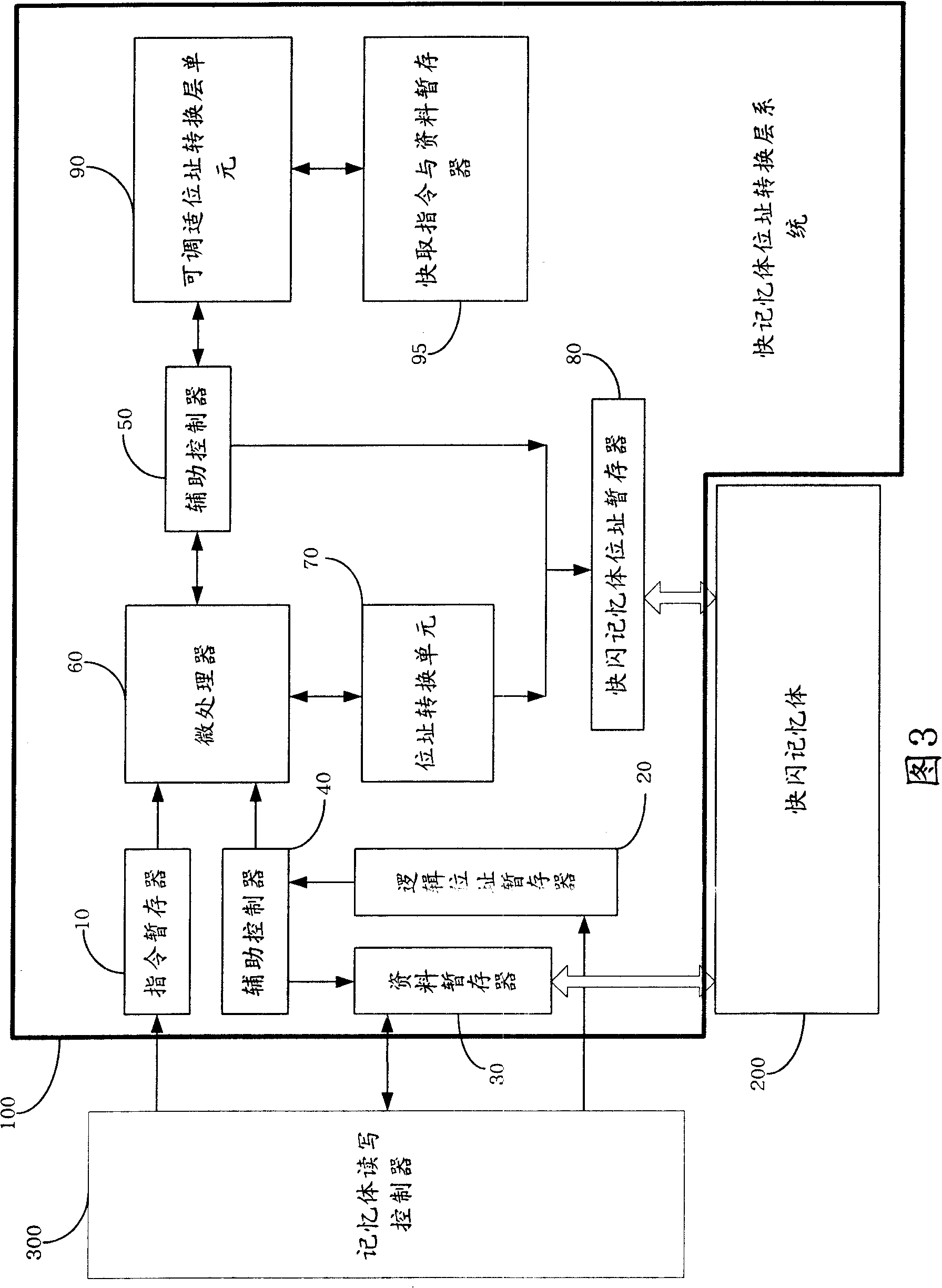
[0051] Please refer to Fig. 3 first, the flash memory changing layer system 100100 of the present invention is to connect between a flash memory 200 and a memory read-write controller 300, and the memory read-write controller 300 is an existing flash memory card reader or a personal computer. card interface, wherein, the cache device 100 includes an instruction cache 10, a logical address cache 20, a data cache 30, a pair of auxiliary controllers 40 and 50, a microprocessor 60, an address translation unit 70, and a flash memory address cache device 80, an adjustable address translation layer unit 90, and a cache instruction and data buffer 95. The instruction register 10 is connected to the memory read / write controller 300 to receive the flash memory 200 data read / write sent by the memory read / write controller 300. command and store it temporarily.

[0052] The above-mentioned logical address register 20 is connected to the memory read / write controller 300 to receive and tempo...


PUM


Abstract

A flash memory address translation layer system connected with a flash memory and an EMS read/write controller comprises: an instruction buffer for connecting with the EMS memory read/wrote controller; a logical address buffer for connecting the EMS memory read/wrote controller; a data buffer for connecting with the EMS memory and the EMS memory read/wrote controller; a pair of assistant controller for providing an instruction assistant function for controlling data's read/write; a microprocessor for connecting the instruction buffer and two assistant controllers; an address translation unit for connecting the microprocessor; a flash memory address buffer for connecting with the assistant controller, address translation unit and the flash; a adjustable address translation layer unit for connecting with an assistant controller; a quick fetch instruction and data buffer for connecting with the adjustable address translation unit. The invention can greatly reduce the number of invalid data collection and occupy capacity of the flash memory, and has a quick mechanism with space efficiency to improve and quicken the efficiency which the logical address corresponds to the real flash address.

Description

technical field [0001] The present invention relates to one, in particular to a flash memory address translation layer system. Background technique [0002] Flash memory is widely used in computer hosts or consumer electronics products, such as flash memory in existing flash drives and MP3 players, which are the most common examples of flash memory applications. However, NAND flash memory (NAND flash memory) is currently widely used For embedded storage systems, flash memory is composed of many pages (Page), each page size is fixed (for example, 512 bytes), and some consecutive pages (for example, 32 pages) can form a block (Block) , due to the characteristics of flash memory, it is not allowed to write to the same page in the same block, unless there is an action to erase the block where the page is located in advance, due to this access feature, it also causes problems in managing flash memory difficulties. [0003] Usually, in order to allow flash memory to operate unde...

Claims


Application Information

Patent Timeline
IPC IPC(8): G06F12/10G06F12/1009
Inventor 郭大维吴晋贤杨政智
Owner GENESYS LOGIC INC
Why Eureka
Try Eureka