

Capacitor structure
A capacitor structure and electrode technology, applied in the direction of electric solid-state devices, circuits, electrical components, etc., can solve the problem of insufficient noise attenuation characteristics, achieve high noise suppression effect, and improve high-frequency characteristics
- Summary
- Abstract
- Description
- Claims
- Application Information
AI Technical Summary
Problems solved by technology
Method used
Image

Examples
Embodiment approach 1
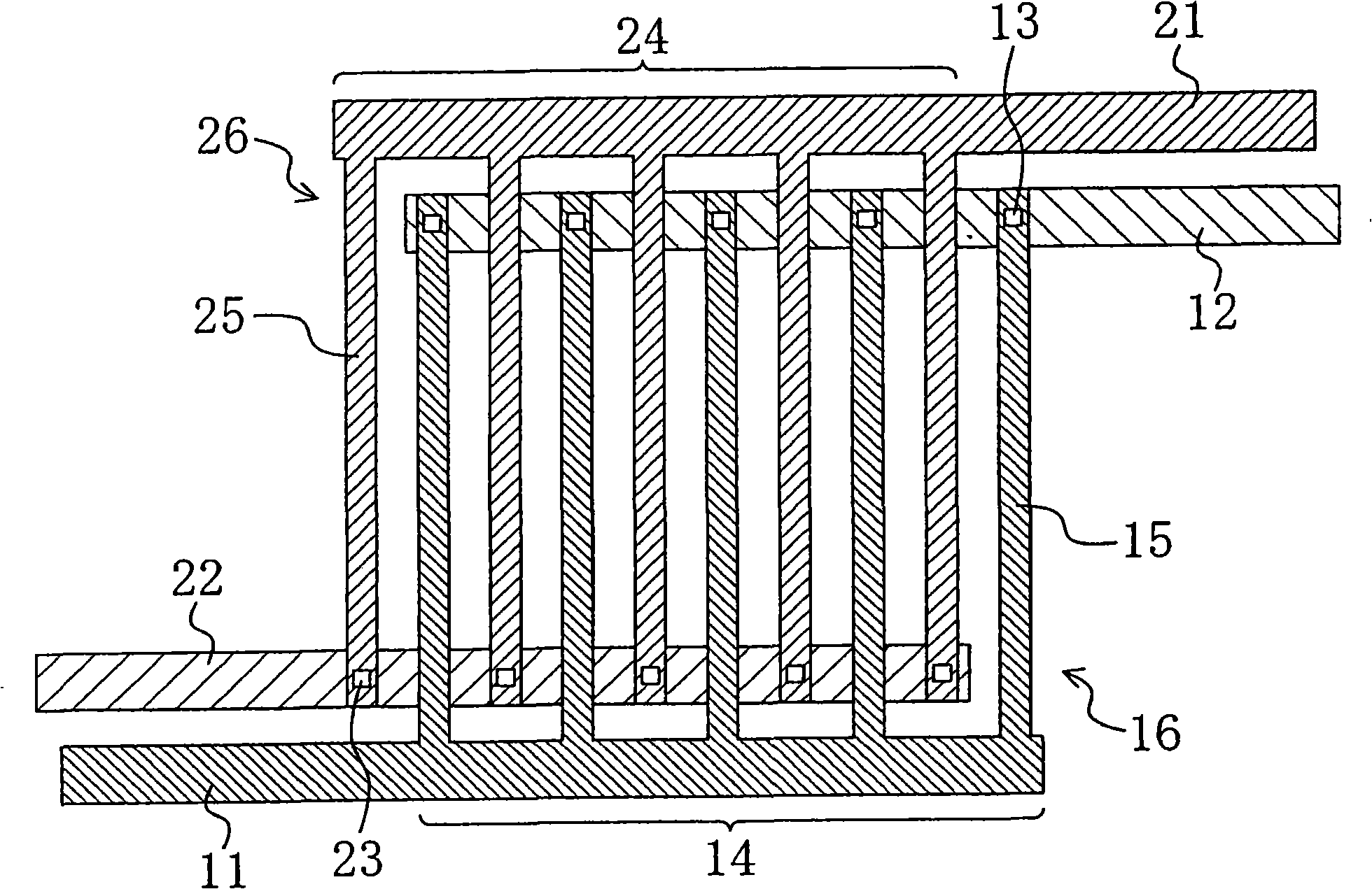
[0027] figure 1 It is a plan view showing the structure of a capacitor formed on an integrated circuit on a semiconductor substrate according to Embodiment 1 of the present invention. figure 1 Among them, 11 and 21 are the first and second electrode wirings formed on the upper wiring layer as the first wiring layer. A first electrode 16 is formed on the first electrode wiring 11 . The first electrode 16 has a plurality of ( figure 1 5 in the middle) tooth portion 15. A second electrode 26 is formed on the second electrode wiring 21 . The second electrode 26 has a plurality of ( figure 1 5 in the middle) tooth portion 25. The first electrode 16 and the second electrode 26 face each other in a state where the tooth portions 15 and 25 are meshed with each other via a dielectric. That is, the first electrodes 16 and the second electrodes 26 have a so-called interdigitated arrangement.
[0028] Further, the tip of each tooth portion 15 of the first electrode 16 is electrical...
Embodiment approach 2
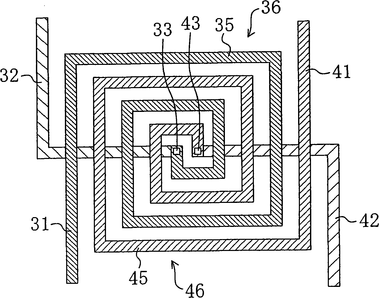
[0035] figure 2 It is a plan view showing a structure of a capacitor formed on an integrated circuit on a semiconductor substrate according to Embodiment 2 of the present invention. figure 2 The shown capacitor structure is to figure 1 In the shown capacitor structure of Embodiment 1, the comb-shaped electrodes are replaced by scroll-shaped electrodes.
[0036] figure 2 Among them, 31, 41 are the first and second electrode wirings formed on the upper wiring layer as the first wiring layer. A first electrode 36 is formed on the first electrode wiring 31 . The first electrode 36 has a scroll portion 35 extending from the first electrode wiring 31 . A second electrode 46 is formed on the second electrode wiring 41 . The second electrode 46 has a scroll portion 45 extending from the second electrode wiring 41 . The first electrode 36 and the second electrode 46 face each other in a state in which the scroll portions 35 , 45 are intertwined with each other via a dielectric...
Embodiment approach 3
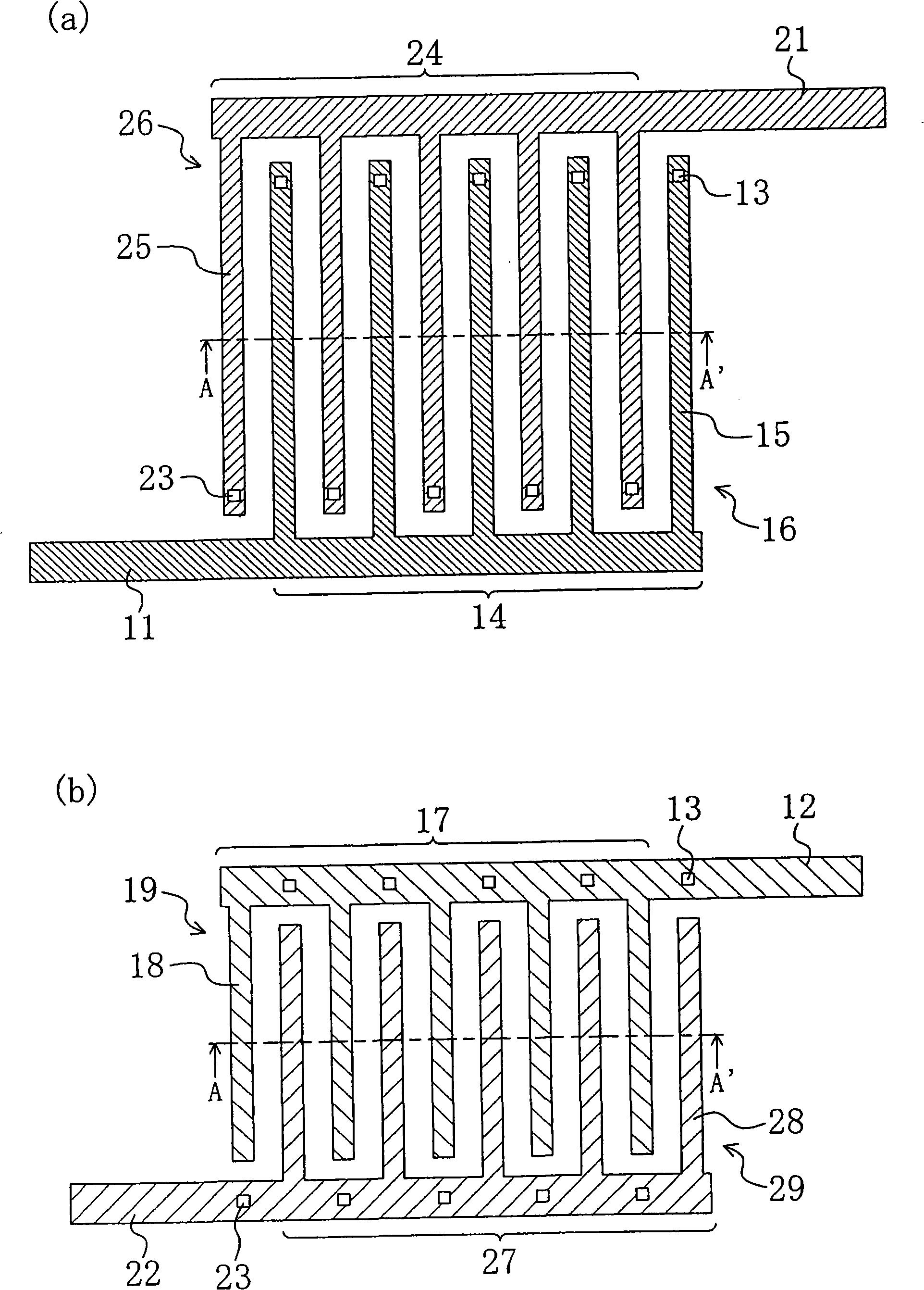
[0044] image 3 It is a plan view showing a capacitor structure formed on an integrated circuit on a semiconductor substrate according to Embodiment 3 of the present invention, in which (a) shows a planar structure of an upper wiring layer, and (b) shows a planar structure of a lower wiring layer. and also, Figure 4 yes image 3 The cross-sectional view of the line A-A'.
[0045] image 3 and Figure 4 The capacitor structure with figure 1 The capacitor structure is the basic configuration, and furthermore, a capacitor is formed by opposing electrodes in the lower wiring layer and between the upper and lower wiring layers.
[0046] Such as image 3 As shown, a first electrode 16 and a second electrode 26 are formed on the upper wiring layer. The first electrode 16 has a plurality of teeth 15 protruding from the electrode base 14 of the first electrode wiring 11 in a comb shape, and the second electrode 26 has a plurality of teeth protruding from the electrode base 24 o...
PUM
 Abstract
Description
Claims
Application Information