Method for manufacturing non-volatile microelectromechanical memory unit

A memory unit, non-volatile technology, applied in the direction of static memory, digital memory information, manufacturing microstructure devices, etc., can solve problems such as difficult design and manufacture of embedded non-volatile memory devices, to achieve accurate switching voltage, The effect of improving performance

Inactive Publication Date: 2011-07-20
QORVO US INC
View PDF0 Cites 0 Cited by
  • Summary
  • Abstract
  • Description
  • Claims
  • Application Information

AI Technical Summary

Problems solved by technology

Therefore, it is more difficult to design and manufacture embedded non-volatile memory devices due to their smaller size and manufacturing requirements

Method used


Image

  • Method for manufacturing non-volatile microelectromechanical memory unit
  • Method for manufacturing non-volatile microelectromechanical memory unit
  • Method for manufacturing non-volatile microelectromechanical memory unit

Examples


Embodiment Construction

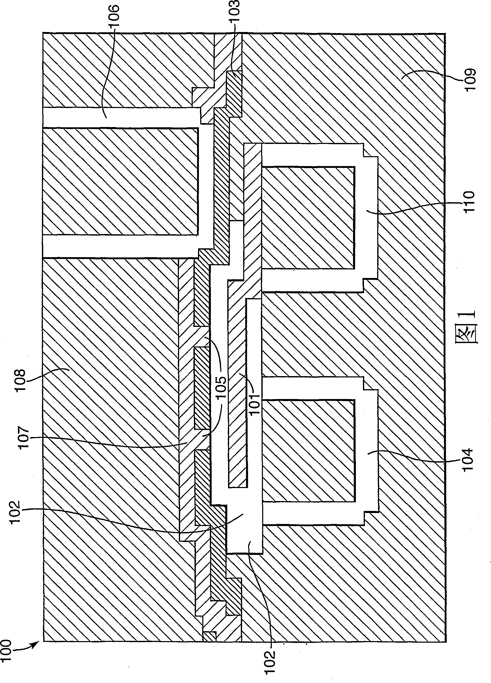
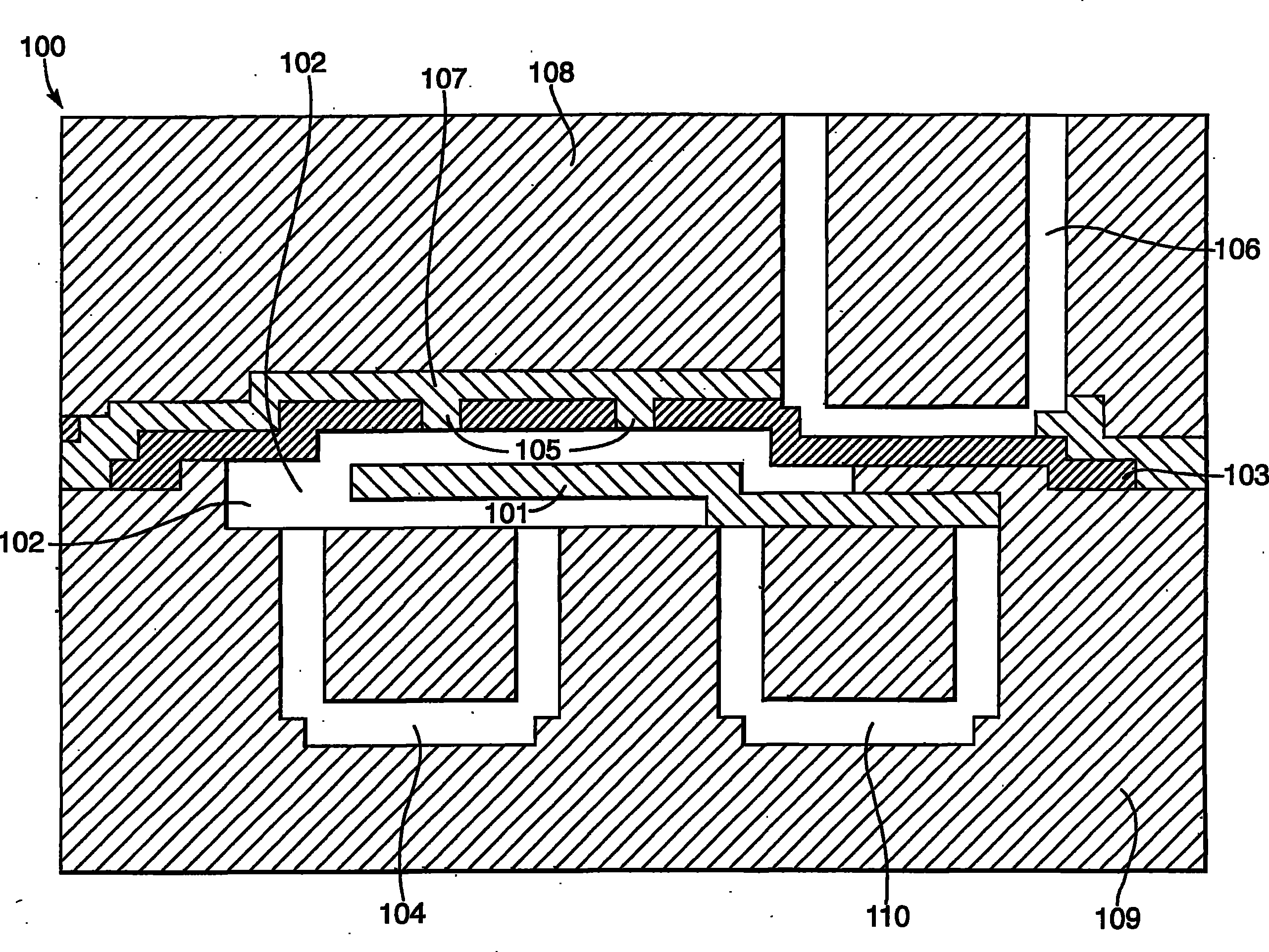
[0033] see figure 1 , the first example of the present invention will now be described. In the first example, device 100 is a scaled-down version of a microelectromechanical cantilever device, fabricated in part by atomic layer deposition (ALD). The first dielectric material layer 109 includes a pull-down electrode 104 and a cantilever electrode 110 .

[0034] On this dielectric material layer 109, a cantilever 101 surrounded by a sacrificial material (not shown) is formed by alternately depositing a sacrificial material and a cantilever material. A conductive material layer 103 is then deposited over the second sacrificial material layer. Two release holes 105 are then etched in the conductive layer 103 . Next, sacrificial material is etched through the release hole 105 . When the sacrificial material is etched away, a cavity 102 is formed in which the cantilever 101 is suspended.

[0035] An insulating layer 107 is then deposited over the conductive layer 103, which act...


PUM


Abstract

A non-volatile memory device and method of manufacturing a non-volatile micro-electromechanical memory cell. The method comprises the first step of depositing a first layer of sacrificial material on a substrate by use of Atomic Layer Deposition. The second step of the method is providing a cantilever (101) over at least a portion of the first layer of sacrificial material. The third step is depositing, by use of Atomic Layer Deposition, a second layer of sacrificial material over the first layer of sacrificial material and over a portion of the cantilever such that a portion of the cantilever is surrounded by sacrificial material. The fourth step is providing a further layer material (107) which covers at least a portion of the second layer of sacrificial material. Finally, the last stepis etching away the sacrificial material surrounding the cantilever, thereby defining a cavity (102) in which the cantilever is suspended.

Description

technical field [0001] The present invention is directed to the field of non-volatile memory (NVM) devices. There are several known types of stand-alone NVM devices. One type of NVM that offers several advantages is a cantilevered microelectromechanical system (MEMS) device. Background technique [0002] The use of MEMS devices results in better memory performance and simpler process integration and fabrication, thereby reducing production costs. However, in order to implement MEMS-based NVM in front-line processes for fabricating integrated devices, current cantilever-based switches need to be significantly scaled down. Because MEMS-based NVMs are mechanical in nature, they are difficult to scale down for integrated devices. [0003] The lateral dimensions of MEMS devices can be readily scaled using known photolithographic processes. However, vertical scaling involves providing very thin mechanical and sacrificial layers. Providing these layers poses several problems r...

Claims


Application Information

Patent Timeline
Patent Type & Authority Patents(China)
IPC IPC(8): B81B3/00G11C23/00G11C11/50H01H1/00B81C1/00H01H51/12H01H59/00
CPCG11C23/00B81C2201/0176B81C1/0015B81C2201/014H01H51/12H01H59/0009
Inventor 罗伯特·凡·坎彭罗伯特·考津齐
Owner QORVO US INC
Why Eureka
Try Eureka