

Field emission backlight
A technology of backlight source and field emission, applied in the field of backlight source, can solve the problems of uneven light emission and uneven output light of the phosphor layer thickness and electron phosphor layer.
- Summary
- Abstract
- Description
- Claims
- Application Information
AI Technical Summary
Problems solved by technology
Method used
Image

Examples
Embodiment Construction
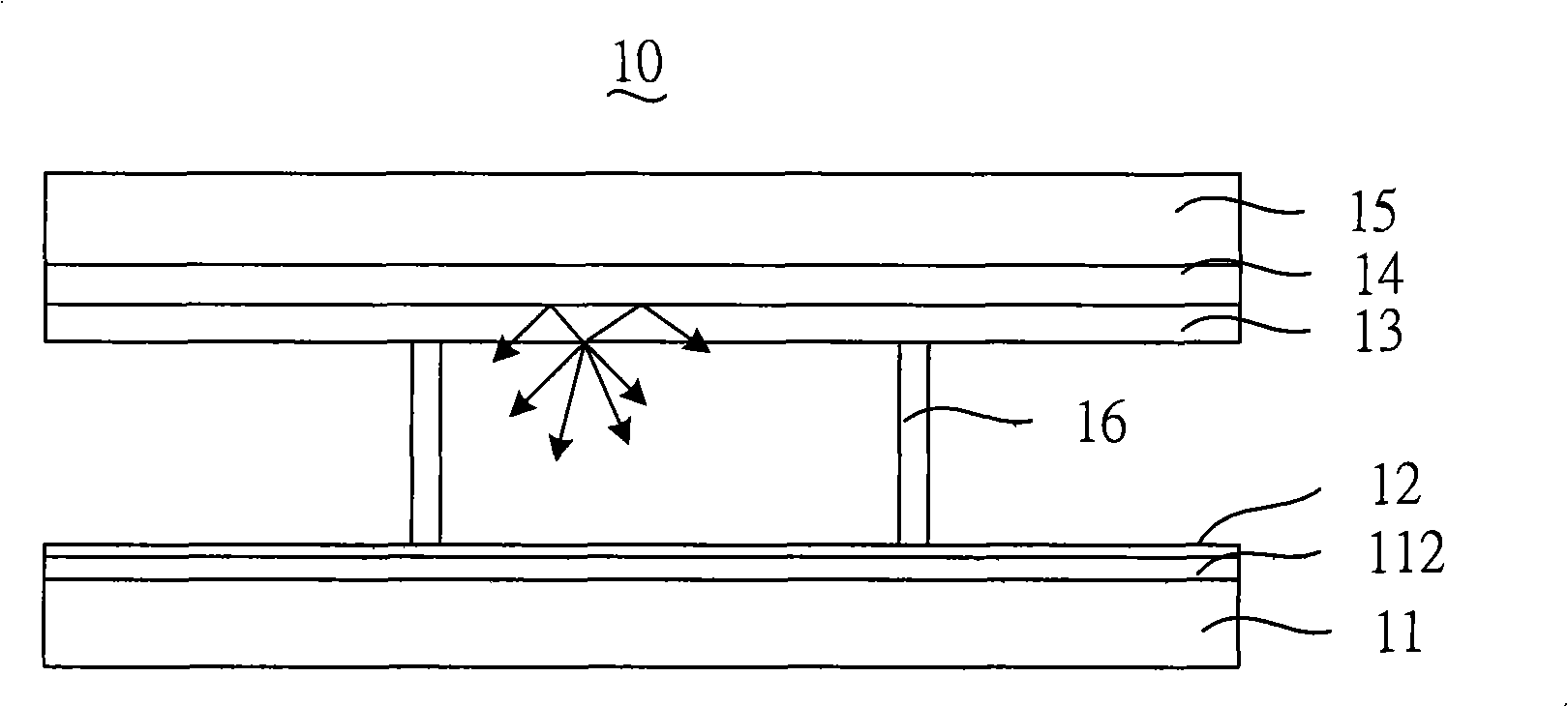
[0014] refer to figure 1 The field emission backlight 10 of the first embodiment of the technical solution includes a cathode substrate 11 , a transparent conductive layer 112 , a cathode 12 , a fluorescent layer 13 , a light reflection layer 14 , an anode substrate 15 and a support bar 16 .
[0015] The cathode substrate 11 is opposite to the anode substrate 15 . The support bar 16 is disposed between the cathode substrate 11 and the anode substrate 15 to form a space between the cathode substrate 11 and the anode substrate 15 . Since a vacuum is drawn between the cathode substrate 11 and the anode substrate 15, the support bar 16 must be made of a material with higher strength, such as metal or ceramics.
[0016] The cathode substrate 11 is formed of a transparent material, such as a transparent glass plate. The transparent conductive layer 112 may be an indium tin oxide thin film, which is disposed on the surface of the cathode substrate 11 near the anode substrate 15 . ...
PUM
| Property | Measurement | Unit |
|---|---|---|
| thickness | aaaaa | aaaaa |
| melting point | aaaaa | aaaaa |
Abstract
Description
Claims
Application Information