Method and device for decreasing offset voltage of Hall integrated circuit

An offset voltage, integrated circuit technology, applied in circuits, electrical components, electro-solid devices, etc., can solve problems such as unpredictable and control offset voltage, and achieve good consistency, small Hall output voltage offset, and good matching. Effect

Inactive Publication Date: 2008-10-22
WUXI POWERSILICON TECH
View PDF0 Cites 15 Cited by
  • Summary
  • Abstract
  • Description
  • Claims
  • Application Information

AI Technical Summary

Problems solved by technology

But in practice even with the figure 2 The layout design of the symmetrical array Hall cel

Method used


Image

  • Method and device for decreasing offset voltage of Hall integrated circuit
  • Method and device for decreasing offset voltage of Hall integrated circuit
  • Method and device for decreasing offset voltage of Hall integrated circuit

Examples


no. 1 example

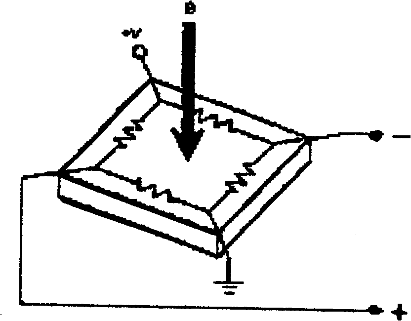
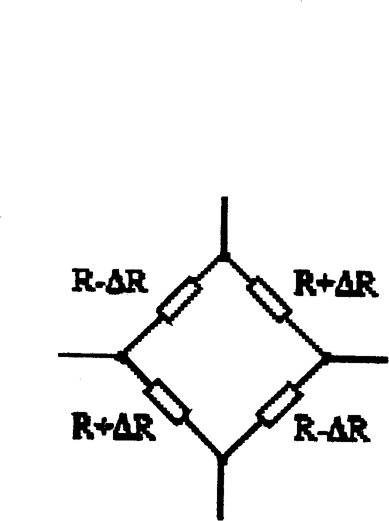
[0033] Image 6 gives Figure 5 A cross-sectional view along the A-A direction. The same number in the figure represents the same area. A lightly doped N-type epitaxial layer 2 is grown on a semiconductor P-type base substrate 1 , and the epitaxial layer 2 is separated by heavily doped P-type isolation bands 3 into isolated epitaxial islands, that is, Hall cells 4 . Four Hall cells 4 that are exactly the same and connected in parallel form a Hall sensor and are located in the middle of the chip ( Figure 5 ).

no. 2 example

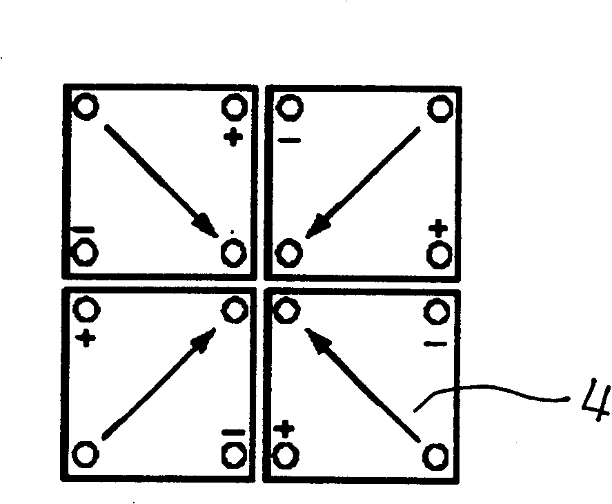
[0035] Figure 8 The layout design method and connection method of the Hall unit 4 in the second embodiment are given. Compared with the first embodiment, the Hall unit 4 is set at an angle of 45 degrees, and the wider epitaxial layer is not drawn in the figure 2 and the barrier 3.

no. 3 example

[0037] Figure 9 The layout design method and connection method of the Hall unit 4 in the third embodiment are given. Compared with the second embodiment, it consists of only three Hall units 4, and the Hall units 4 are symmetrically arranged in a parallelogram center. , the wider epitaxial layer 2 and the isolation zone 3 are not shown in the figure.


PUM


Abstract

The invention relates to a method for reducing the misalignment voltage of a hall integrated circuit. The method is as follows: a hall unit array is positioned on the central part of a chip and other circuit devices which serve hall units are arranged on the circumference of the hall unit array and in parallel connection with the hall units; the circumference of each hall unit is enclosed by an isolation belt and an epitaxial layer which are formed by heavy doping; involved devices comprise a semiconductor P type substrate and a light-dope semiconductor N type epitaxial layer which is grown on the semiconductor P type substrate; a heavy-dope semiconductor P type isolation belt is also arranged on the semiconductor N type epitaxial layer; and the isolation belt divides the semiconductor N type epitaxial layer into at least three isolated hall units which are centrally symmetrically arranged arrays. The method can make affection of stress, pressure and so on of the chip edge on the hall devices be consistent, make affection of other devices on the circumference of the hall units on the misalignment voltage of the hall units smaller, make affection of deviation of the manufacturing technique on the hall units be consistent, and have better matching property.

Description

【Technical field】 [0001] The present invention relates to the improvement of semiconductor integrated circuits, especially Hall devices. More specifically, it relates to a layout design method and device for reducing the offset voltage of a Hall device integrated in an integrated circuit. 【Background technique】 [0002] Hall devices based on the principle of the Hall effect are mainly used as magnetic sensors. As we all know, the advantage of Hall devices made of silicon materials is that their manufacturing technology is compatible with microelectronic integrated circuit technology, and can be combined with various protection circuits (such as adjustment, compensation and protection circuits) and signal processing circuits (such as amplifiers, Schmitt trigger, band-pass filter and output circuit) etc. are integrated together to form various functional circuits, realizing mass production and greatly reducing production costs; output signals can be directly used by computers...

Claims


Application Information

Patent Timeline
IPC IPC(8): H01L27/22
Inventor 管慧陈俊
Owner WUXI POWERSILICON TECH
Why Eureka
Try Eureka