Circuit structure and method capable of reducing oscillation of semiconductor circuit for power conversion

A technology for converting circuits and semiconductors, which is applied in the direction of output power conversion devices, DC power input conversion to DC power output, and conversion equipment without intermediate conversion to AC power.

Inactive Publication Date: 2008-10-22
ALPHA & OMEGA SEMICON LTD
View PDF0 Cites 13 Cited by
  • Summary
  • Abstract
  • Description
  • Claims
  • Application Information

AI Technical Summary

Problems solved by technology

However, this means that other switching losses and reduced inductance wi

Method used


Image

  • Circuit structure and method capable of reducing oscillation of semiconductor circuit for power conversion
  • Circuit structure and method capable of reducing oscillation of semiconductor circuit for power conversion
  • Circuit structure and method capable of reducing oscillation of semiconductor circuit for power conversion

Examples


Embodiment Construction

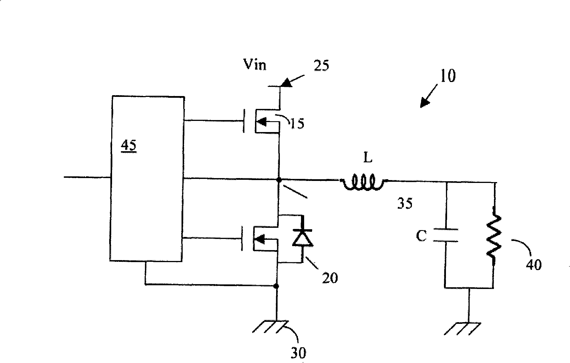
[0042] enter figure 2 Shown in A is a schematic diagram of the circuit structure of the voltage converter 100 of the present invention. Similar to the voltage converter 10 in the background art, the voltage converter 100 includes a high-side MOSFET 105, which is presented with a body diode 108 and a low-side MOSFET 100, which Accompanied by a body diode 112 present. The drain terminal of the low-side MOSFET 110 is connected to the source of the high-side MOSFET 105 at a central connection point 115 . The method for reducing the ringing oscillation is to prevent the loop reverse recovery energy of the body diode 112 from passing through the parasitic inductance such as Lser and the parasitic capacitance. This is achieved by reversing most of the reverse current back to the DC input supply, which is connected to the drain terminal of the high side Mosfet 105 and the source terminal of the low side Mosfet 110 . To achieve this purpose, the fast-start diode 120 represented by ...


PUM


Abstract

The invention discloses a conversion device which comprises a high side metal oxide semiconductor field effect transistor (MOSFET) chip provided with a first high side source which is connected to a low side drain of a low side metal oxide semiconductor field effect transistor chip. The conversion device also comprises a transient reverse current transfer circuit which is connected to a drain of a low side metal oxide semiconductor field effect transistor chip to transfer a reverse transient current so as to transfer a reverse transient current passing through one body diode of the low side metal oxide semiconductor field effect transistor chip when the low side metal oxide semiconductor field effect transistor chip is closed, and to reduce the vibration of transient ringing. The reverse transient current transfer circuit comprises a diode which is used to guide a reverse transient current from the drain. The reverse transient transfer circuit also comprises a capacitor which is connected between the diode and the low side metal oxide semiconductor field effect transistor chip.

Description

technical field [0001] The present invention relates to a circuit design and a structure of a semiconductor power device, such as a metal-oxide-semiconductor field-effect transistor-based device, in particular to a novel and improved circuit structure design and assembly method, which can reduce Ringing of semiconductor power devices such as synchronous converters or switching circuits. Background technique [0002] Conventional power MOSFET devices have struggled with ringing oscillations that can lead to shooting through problems. Ringing and shooting through problems cause excessive waste and loss of efficiency, especially in conversions such as synchronous buck converters, halfbridge converters or inverters In the circuit are two power metal-oxide-semiconductor field-effect transistors with complementary design for switching. Two MOSFETs connected in series across a voltage source are generally referred to as high-side and low-side (LS) MOSFETs, respectively. The low-...

Claims


Application Information

Patent Timeline
IPC IPC(8): H02M3/10H02M3/155
Inventor 杉杰・哈瓦娜
Owner ALPHA & OMEGA SEMICON LTD
Why Eureka
Try Eureka