Semiconductor device and manufacturing method thereof

A manufacturing method and semiconductor technology, applied in semiconductor/solid-state device manufacturing, semiconductor devices, semiconductor/solid-state device components, etc., can solve problems such as peeling and affecting the quality of wire bonding, so as to improve tensile strength and avoid thermal expansion reaction , Reduce the effect of mechanical influence

Active Publication Date: 2010-09-29
SEMICON MFG INT (SHANGHAI) CORP
View PDF6 Cites 0 Cited by
  • Summary
  • Abstract
  • Description
  • Claims
  • Application Information

AI Technical Summary

Problems solved by technology

However, after thermal annealing, during the wire bonding process using the aluminum pad, the phenomenon that the pad 17 and the copper interconnection line dual damascene interconnection line 13 are often peeled off, such as figure 2 shown
This situation can seriously affect the quality of the wire bond

Method used


Image

  • Semiconductor device and manufacturing method thereof
  • Semiconductor device and manufacturing method thereof
  • Semiconductor device and manufacturing method thereof

Examples


Embodiment Construction

[0035] In order to make the above objects, features and advantages of the present invention more comprehensible, specific implementations of the present invention will be described in detail below in conjunction with the accompanying drawings.

[0036] In the following description, numerous specific details are set forth in order to provide a thorough understanding of the present invention. However, the present invention can be implemented in many ways other than those described here, and those skilled in the art can make similar extensions without departing from the connotation of the present invention. Accordingly, the invention is not limited to the specific implementations disclosed below.

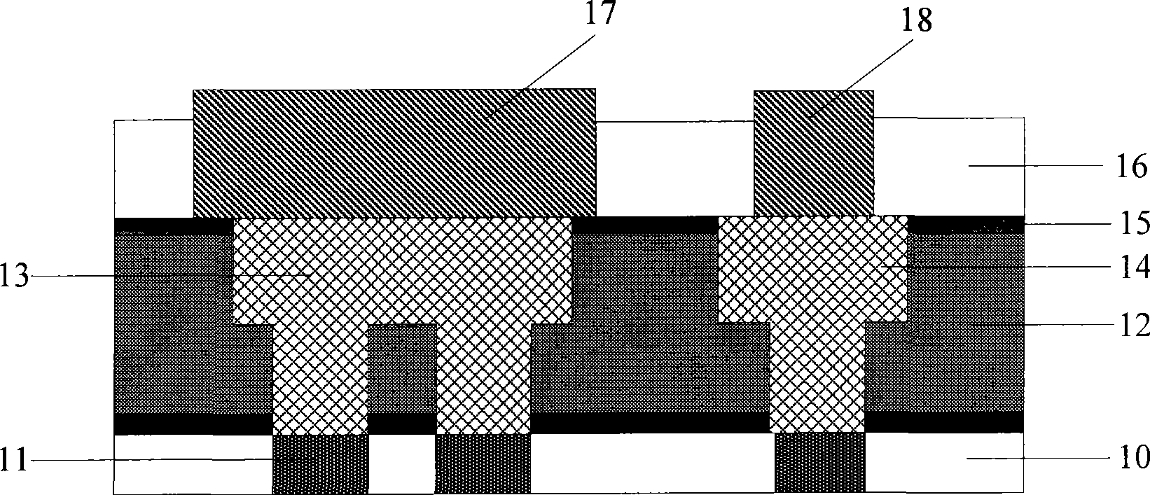
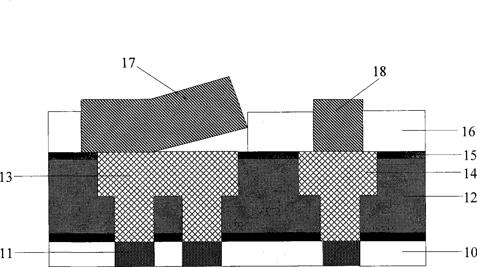
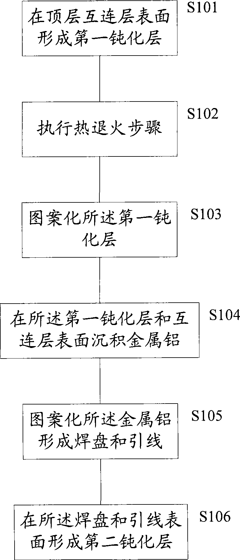
[0037] image 3 It is a flow chart of the semiconductor device manufacturing method of the present invention, such as image 3 As shown, the manufacturing method of the semiconductor device of the present invention first forms a first passivation layer on the surface of the top inter...


PUM

PropertyMeasurementUnit
thicknessaaaaaaaaaa

Abstract

A semiconductor apparatus and a manufacture method thereof include the following steps of: forming a first passivation layer on the surface of the interconnection layer of a top layer; carrying out the step of hot annealing; patterning the first passivation layer; depositing metal aluminum on the first passivation layer and the surface of the interconnection layer; patterning the metal aluminum to form a bonding pad and a down-lead; forming a second passivation layer on the bonding pad and the surface of the down-lead; the invention can effectively avoid the peeling-off phenomenon of the interconnection line of an aluminum bonding pad and copper when bonding the down-lead.

Description

technical field [0001] The invention relates to the technical field of semiconductor manufacturing, in particular to a semiconductor device and a manufacturing method thereof. Background technique [0002] Today's semiconductor device manufacturing technology is developing rapidly, semiconductor devices already have a deep submicron structure, and integrated circuits contain a huge number of semiconductor components. In such large-scale integrated circuits, high-performance, high-density connections between components are not only interconnected in a single interconnect layer, but also interconnected between multiple layers. Therefore, a multilayer interconnection structure is usually adopted, especially a multilayer interconnection structure formed by a dual-damascene process, which preforms a trench (trench) and a connection hole (via) in the interlayer dielectric layer, The trenches and connection holes are then filled with a conductive material such as copper (Cu). see...

Claims


Application Information

Patent Timeline
Patent Type & Authority Patents(China)
IPC IPC(8): H01L23/485H01L21/60
CPCH01L24/05H01L2224/02166H01L2224/03001H01L2924/14H01L2924/351
Inventor 宁先捷
Owner SEMICON MFG INT (SHANGHAI) CORP
Why Eureka
Try Eureka