
Copper-clad ceramic substrate with high bonding strength and preparation process thereof

A copper-clad ceramic substrate and preparation process technology, which is applied in the processing of insulating substrates/layers, printed circuit manufacturing, printed circuits, etc. Uniformity, affecting the activity of reagents, etc., to avoid the production of copper sulfate, reduce the depth of brush marks, and shorten the time of micro-etching

Active Publication Date: 2022-04-29
南通威斯派尔半导体技术有限公司
View PDF15 Cites 0 Cited by
  • Summary
  • Abstract
  • Description
  • Claims
  • Application Information

AI Technical Summary

Problems solved by technology

The solder mask layer is set on the circuit and the base material of the PCB that do not need to be soldered to prevent bridging between the lines during soldering, resulting in short circuit, and to prevent mechanical damage, provide a permanent electrical environment, resist chemical protection, and maintain good insulation on the board surface Performance performance; after the copper base is sintered at high temperature, there will be deep oxidation and carbon migration on the copper surface. Before the preparation of the solder mask layer, the copper-clad ceramic substrate needs to be pretreated to remove oxides on the surface of the copper base and keep the board surface clean; The existing method is generally to use mechanical removal such as grinding and brushing. The mechanical method will damage the copper surface and cause a layer of brush marks on the copper surface. During the process, the increase of copper ions will precipitate copper sulfate to affect the activity of the reagent, and the resulting grains will appear finer and uneven due to insufficient microetching, which will have a negative impact on the bonding strength between the solder mask and the copper base.

Method used


Image

  • Copper-clad ceramic substrate with high bonding strength and preparation process thereof
  • Copper-clad ceramic substrate with high bonding strength and preparation process thereof

Examples

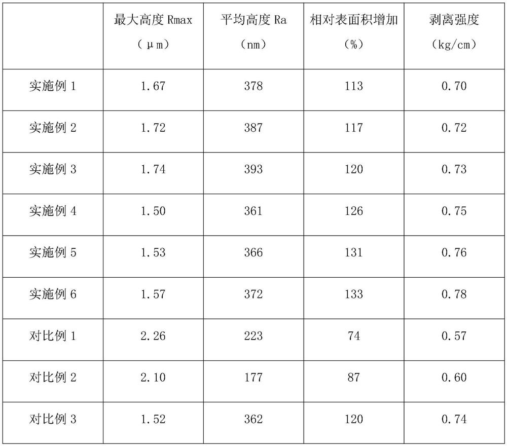

Embodiment 1

[0037] (1) Grinding plate: Use ceramic brush and cloth brush to polish the copper-clad ceramic substrate in turn; the mesh number of the ceramic brush is 600 mesh, the thickness of the ceramic sheet is 8mm, the speed selection is 2.5m / min, and the brushing current is 2.7 A; The weaving brush is 400 mesh, the speed is 2.5m / min, and the brushing current is 2.9A;

[0038] Spray washing: clean the copper powder produced by the grinding plate, and recycle the copper powder;

[0039] Pickling: Use 98% concentrated sulfuric acid, 5-aminotetrazole, nickel sulfate, and 30% hydrogen peroxide to prepare a pickling agent, and clean the copper base at a temperature of 32°C to remove surface oxides;

[0040]Alkaline cleaning: Use sodium hydroxide aqueous solution to clean the copper base at 37°C to remove surface grease, fingerprints, slight oxidation and other organic pollutants, and at the same time form an oxide film, which is beneficial to accelerate the copper base surface to the organ...

Embodiment 2

[0043] (1) Grinding plate: Use ceramic brush and cloth brush to polish the copper-clad ceramic substrate in turn; the mesh number of the ceramic brush is 500 mesh, the thickness of the ceramic sheet is 8mm, the speed selection is 2.5m / min, and the brushing current is 2.7 A; The weaving brush is 50 mesh, the speed is 2.5m / min, and the brushing current is 2.9A;

[0044] Spray washing: clean the copper powder produced by the grinding plate, and recycle the copper powder;

[0045] Pickling: Use 98% concentrated sulfuric acid, 5-aminotetrazole, nickel sulfate, and 30% hydrogen peroxide to prepare a pickling agent, and clean the copper base at a temperature of 35°C to remove surface oxides;

[0046] Alkaline cleaning: Use sodium hydroxide aqueous solution to clean the copper base at 40°C to remove surface grease, fingerprints, slight oxidation and other organic pollutants, and at the same time form an oxide film, which is beneficial to accelerate the reaction of organic matter on th...

Embodiment 3

[0049] (1) Grinding plate: Use ceramic brush and cloth brush to polish the copper-clad ceramic substrate in turn; the mesh number of the ceramic brush is 400 mesh, the thickness of the ceramic sheet is 8mm, the speed selection is 2.5m / min, and the brushing current is 2.7 A; The weaving brush is 400 mesh, the speed is 2.5m / min, and the brushing current is 2.9A;

[0050] Spray washing: clean the copper powder produced by the grinding plate, and recycle the copper powder;

[0051] Pickling: Use 98% concentrated sulfuric acid, 5-aminotetrazole, nickel sulfate, and 30% hydrogen peroxide to prepare a pickling agent, and clean the copper base at a temperature of 38°C to remove surface oxides;

[0052] Alkaline cleaning: Use sodium hydroxide aqueous solution to clean the copper base at 43°C to remove surface grease, fingerprints, slight oxidation and other organic pollutants, and form an oxide film at the same time, which is beneficial to accelerate the copper base surface to the orga...


PUM

PropertyMeasurementUnit
Meshaaaaaaaaaa
Thicknessaaaaaaaaaa
Meshaaaaaaaaaa

Abstract

The invention discloses a copper-clad ceramic substrate with high bonding strength and a preparation process thereof. The preparation process comprises the following steps: (1) grinding a plate: grinding the copper-clad ceramic substrate by using a ceramic brush and a weaving brush in sequence; and (2) micro-etching: treating the copper-clad ceramic substrate polished by the micro-etching liquid. The micro-etching time is shortened by modifying the mesh number of the polish-brush wheel, reducing the brush mark depth and reducing the mechanical influence, generation of copper sulfate is avoided by cooperating with adjustment of the micro-etching liquid, the activity of the micro-etching liquid is improved, a layer of uniform and compact rough surface with moderate depth is formed on the surface of the copper base, crystal grains can be promoted to appear quickly through adjustment of the micro-etching liquid, the crystal grains are more prominent, and the service life of the copper base is prolonged. The crystal grains are thicker and more uniform; and more uniform coarse grains on the surface of the copper base can increase the tensile force of a bonding wire, so that the high bonding strength between the copper-clad ceramic substrate and the solder mask layer is improved.

Description

technical field [0001] The invention relates to the technical field of copper-clad ceramic substrates, in particular to a copper-clad ceramic substrate with high bonding strength and a preparation process thereof. Background technique [0002] Printed Circuit Board (PCB) exists in electronic components and is used to provide mechanical support for fixed assembly, realize wiring and electrical connection or electrical insulation between electronic components, and provide required electrical characteristics. PCB generally includes pads, vias, soldering layers, silk screen layers, copper wires, components and other parts. In order to increase the thickness of the copper skin, the green oil is often drawn on the solder mask layer and tinned. The solder mask layer is set on the circuit and the base material of the PCB that do not need to be soldered to prevent bridging between the lines during soldering, resulting in short circuit, and to prevent mechanical damage, provide a perm...

Claims


Application Information

Patent Timeline
IPC IPC(8): H05K3/28H05K3/00
CPCH05K3/282H05K3/0044H05K3/002
Inventor 俞晓东杨恺刘晓辉
Owner 南通威斯派尔半导体技术有限公司
Learn More