Production method of organic light emitting diode

A technology for light-emitting diodes and a manufacturing method, which is applied in the directions of organic semiconductor devices, semiconductor/solid-state device manufacturing, electrical components, etc., and can solve the problems of uneven light emission and low anode work function.

Active Publication Date: 2008-10-29
INNOCOM TECH (SHENZHEN) CO LTD +1
View PDF0 Cites 10 Cited by
  • Summary
  • Abstract
  • Description
  • Claims
  • Application Information

AI Technical Summary

Problems solved by technology

[0008] In order to solve the shortcomings of low anode work function and non-uniform luminescence of organic light-emitting diodes manufactured by existing manufacturing methods, it is necessary to provide a method for manufacturing organic light-emitting diodes with a higher anode work function and better luminescence uniformity

Method used


Image

  • Production method of organic light emitting diode
  • Production method of organic light emitting diode
  • Production method of organic light emitting diode

Examples


Embodiment Construction

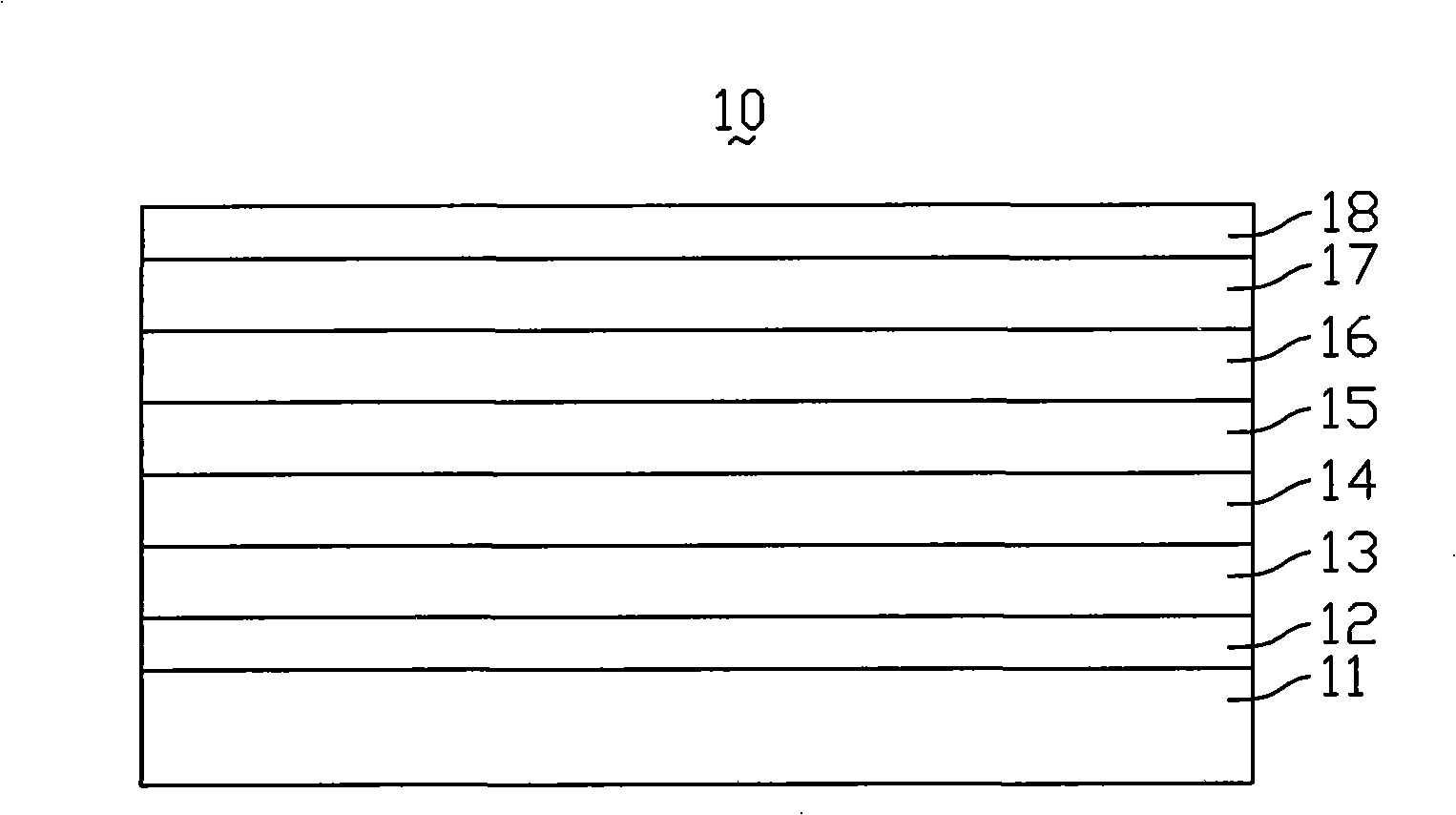
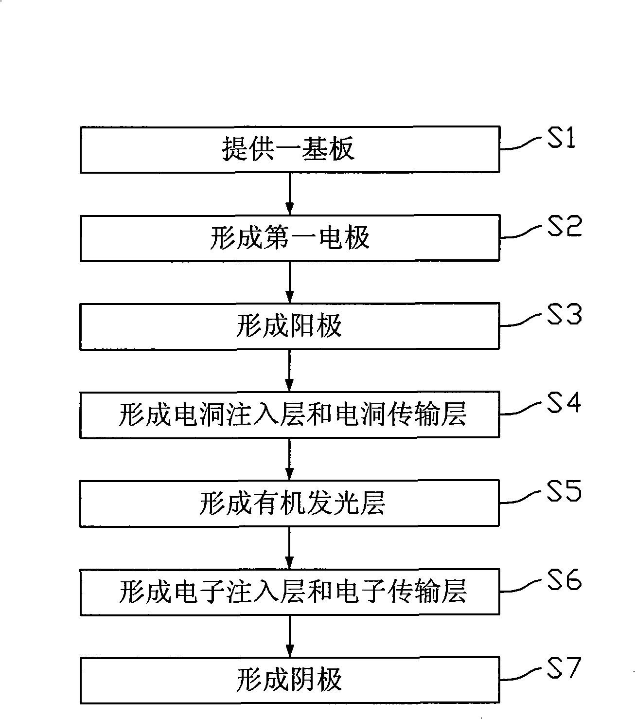
[0014] see image 3 , is a flowchart of a preferred embodiment of the organic light emitting diode manufacturing method of the present invention. The organic light emitting diode manufacturing method includes the following steps: providing a substrate (S1); forming a first electrode (S2); forming an anode (S3); forming a hole injection layer and a hole transport layer (S4); forming an organic light emitting layer ( S5); forming an electron injection layer and an electron transport layer (S6); forming a cathode (S7). The steps are detailed below:

[0015] Step S1, providing a substrate. The provided substrate is used to carry organic light-emitting diodes, and its material can be transparent insulating substances such as glass and quartz.

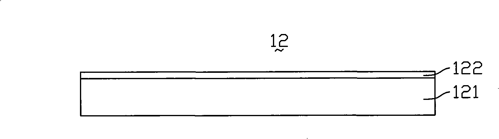
[0016] Step S2, forming a first electrode. A thin layer of indium zinc oxide (Indium Zinc Oxide, IZO) is deposited on the substrate as the first electrode. The thickness of this first electrode can be controlled according to deposition ...


PUM

PropertyMeasurementUnit
thicknessaaaaaaaaaa
thicknessaaaaaaaaaa
thicknessaaaaaaaaaa

Abstract

The invention relates to a manufacture method for an organic light emitting diode, which includes the following steps of: providing an insulated substrate; depositing a conductive thin layer as the first electrode on the insulated substrate; adding oxidizing gas containing oxygen while continuing to deposit the conductive thin layer on the first electrode to form the second electrode, patterning the first and the second electrodes to form an anode; forming an organic light emitting layer on the anode; and forming a cathode on the organic light emitting layer. The manufacture method for the organic light emitting diode can lead the anode work function of the organic light emitting diode to be higher.

Description

technical field [0001] The invention relates to a method for manufacturing an organic light emitting diode (Organic Light Emitting Diode, OLED). Background technique [0002] In recent years, organic light-emitting diodes have attracted the attention of the industry due to their unique advantages, such as simple manufacturing methods, low power consumption, rich colors, and being suitable for flexible substrates and large-area displays. [0003] see figure 1 , is a cross-sectional view of a prior art organic light emitting diode. The organic light emitting diode 10 generally includes a substrate 11, an anode 12, a hole injection layer (Hole Injection Layer, HIL) 13, a hole transport layer (Hole Transfer Layer, HTL) 14 , an organic light emitting layer 15 , an electron transfer layer (Electron Transfer Layer, ETL) 16 , an electron injection layer (Electron Injection Layer, EIL) 17 and a cathode 18 . [0004] The working principle of the organic light emitting diode 10 is a...

Claims


Application Information

Patent Timeline
Patent Type & Authority Applications(China)
IPC IPC(8): H01L51/56
CPCH01L51/0078H01L51/0059H01L51/0038H01L51/0003H01L2251/308H01L51/5206H01L51/001H01L51/0035H01L51/0005H10K71/12H10K71/135H10K71/164H10K85/114H10K85/111H10K85/631H10K85/311H10K50/81H10K50/816H10K2102/103
Inventor 王世昌黄荣龙
Owner INNOCOM TECH (SHENZHEN) CO LTD
Why Eureka
Try Eureka