Gating clock for on-site programmable gate array and implementing method thereof

A gated clock and gate array technology, applied in special data processing applications, instruments, electrical digital data processing, etc., can solve the problems of large occupied area, inability to accurately estimate power consumption, etc., and achieve the effect of reducing area consumption

Inactive Publication Date: 2008-11-12
VIMICRO CORP
View PDF0 Cites 11 Cited by
  • Summary
  • Abstract
  • Description
  • Claims
  • Application Information

AI Technical Summary

Problems solved by technology

[0013] The purpose of the present invention is to provide a gate-controlled clock circuit in a field programmable gate array, so that FPGA can more realistically simulate the gate-controlled clock circuit of ASIC, and solve the occupied area of ​​the gate-controlled clock circuit of ASIC simulated in the prior art Large technical issues that cannot accurately estimate power consumption

Method used


Image

  • Gating clock for on-site programmable gate array and implementing method thereof
  • Gating clock for on-site programmable gate array and implementing method thereof
  • Gating clock for on-site programmable gate array and implementing method thereof

Examples


Embodiment Construction

[0042] In order to make the purpose, technical solutions and advantages of the embodiments of the present invention more clear, specific embodiments will be described in detail below with reference to the accompanying drawings.

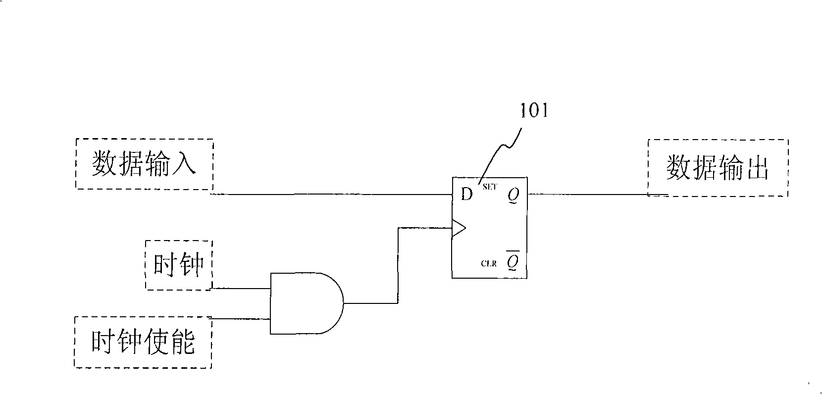
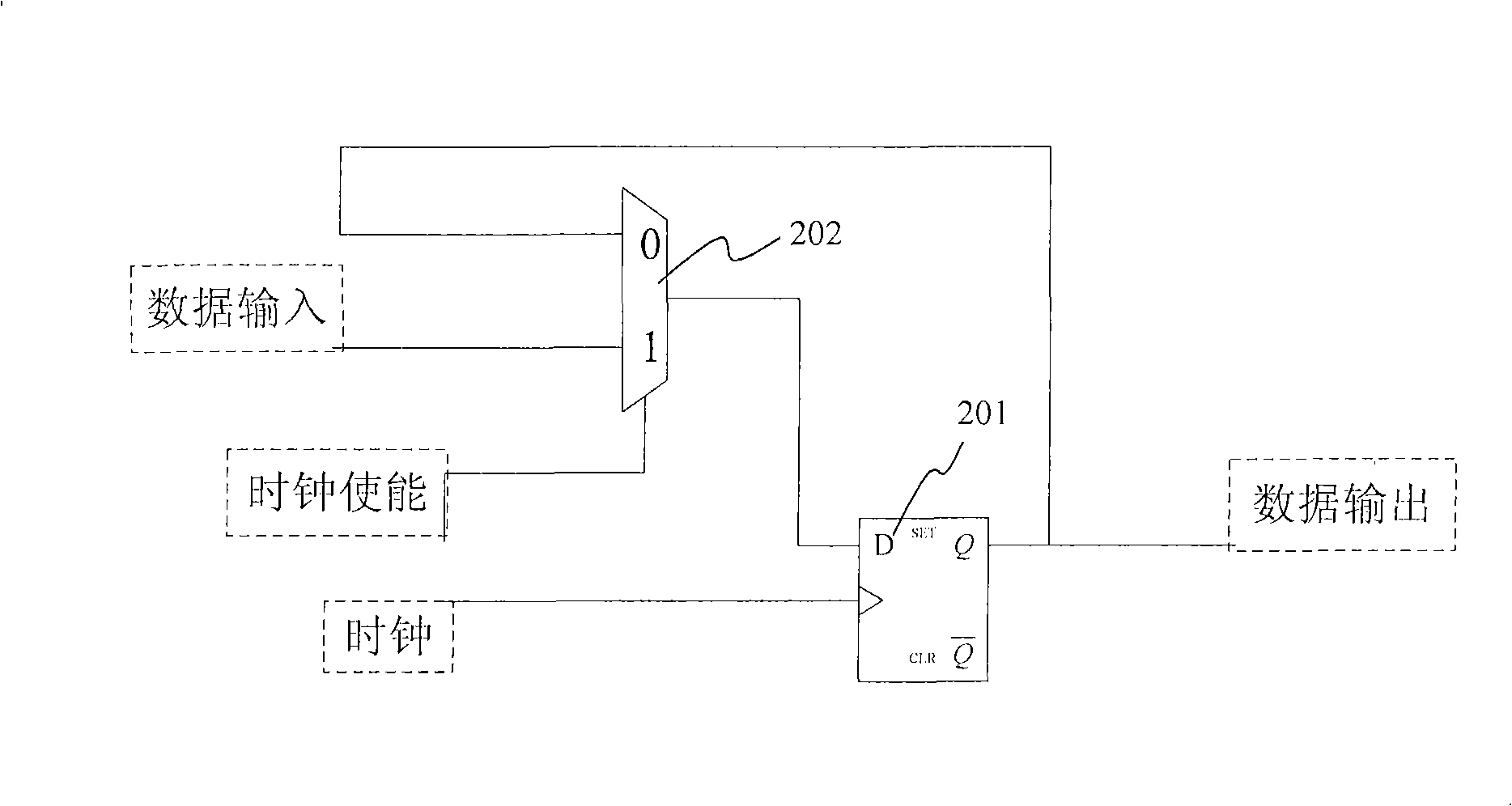
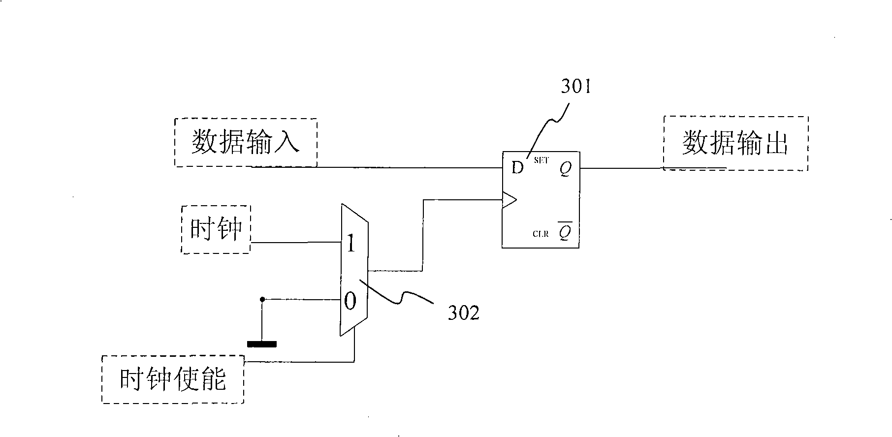
[0043] There is a resource in the FPGA called BUFGMUX (global clock buffer multiplexer). BUFGMUX is not a simple clock buffer. It is a multiplexer with low clock skew, high drive capability and a selector. The BUFGMUX is instantiated using different primitives, and the BUFGMUX can constitute a clock selector, a clock gate, or a simple clock buffer.

[0044] Considering that the FPGA has its own unique clock resources, the embodiments of the present invention will use these resources flexibly and correctly, so as to not only meet the clock tree requirements inside the FPGA, but also satisfy the design verification requirements to the greatest extent.

[0045] image 3The circuit structure diagram of using BUFGMUX to realize the gating clock of FPGA pr...


PUM


Abstract

The invention provides a gated clock in a field programmable gate array and a realizing method thereof; the gated clock includes a plurality of triggers, and a global clock cache multi-route selector the output end of which is connected with the clock input ends of the triggers; the global clock cache multi-route selector is used for leading the input of the clock input ends of the triggers to be a clock signal when a clock enabling signal is effective and leading the input of the clock input ends of the triggers to be zero when the clock enabling signal is ineffective. In the invention, a plurality of triggers are connected with the same BUFGMUX, thereby reducing the consumption of a plurality of areas. The gating mode is consistent with a real ASIC; the clock enabling signal is synchronous with the phase relation of the clock; when the enabling signal is ineffective, the actual clock inputted into the trigger is zero; therefore, more accurate evolution can be carried out on the power consumption; the demands of a clock tree in FPGA can be met; the invention is simple and practical.

Description

technical field [0001] The invention relates to integrated circuit technology, in particular to a gating clock in a field programmable gate array and its realization method. Background technique [0002] In modern integrated circuit design, the size and complexity of chips are increasing exponentially. Especially in the ASIC (Application Specific Integrated Circuits, Application Specific Integrated Circuits) design process, the time spent on verification and debugging accounts for about 70% of the total design period. In order to shorten the time period of verification, on the basis of traditional simulation verification, many new verification methods have emerged, such as assertion verification, coverage-driven verification, and widely used FPGA-based (Field Programmable GateArray, field programmable gate array) prototype verification technology. FPGA prototype verification is the most important verification process before chip tape-out. Compared with simulation software...

Claims


Application Information

Patent Timeline
Patent Type & Authority Applications(China)
IPC IPC(8): G06F17/50
Inventor 邹杨
Owner VIMICRO CORP
Why Eureka
Try Eureka