
Semiconductor device

A semiconductor and device technology, applied in the field of semiconductor devices, can solve problems such as difficulty in improving the avalanche capability of superjunction MOSFETs

Active Publication Date: 2008-11-19
DENSO CORP
View PDF3 Cites 9 Cited by
  • Summary
  • Abstract
  • Description
  • Claims
  • Application Information

AI Technical Summary

Problems solved by technology

Since this avalanche current causes parasitic bipolar transistor action, it is difficult to improve the avalanche capability of super-junction MOSFETs with trench gate structures

Method used


Image

  • Semiconductor device
  • Semiconductor device
  • Semiconductor device

Examples


Embodiment Construction

[0019] A super junction semiconductor device according to a first embodiment of the present invention will be described below with reference to the drawings. For example, the semiconductor device can be used as a switching device of an inverter circuit.

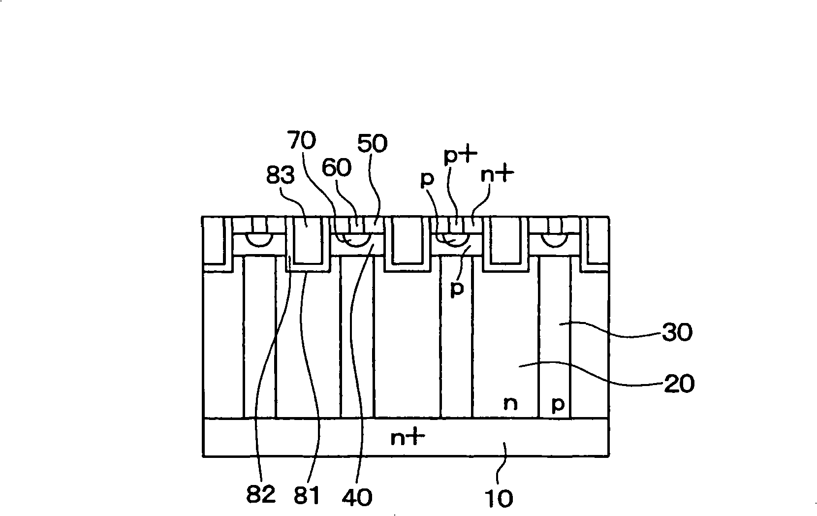
[0020] figure 1 is a diagram showing a cross-sectional view of the semiconductor device according to the first embodiment. Such as figure 1 As shown, a columnar n-type region 20 and a columnar p-type region 30 are formed on the front surface of an n+ type substrate 10 . Columnar n-type regions 20 and columnar p-type regions 30 are alternately arranged in the plane direction of the substrate 10 to form a super junction structure (ie, a super junction layer). Hereinafter, the columnar n-type region 20 and the columnar p-type region 30 are referred to as "n column 20" and "p column 30", respectively.

[0021] Substrate 10 has approximately 1 x 10 19 cm -3 to about 1×10 20 cm -3 impurity concentration. Each of n-column 2...


PUM


Abstract

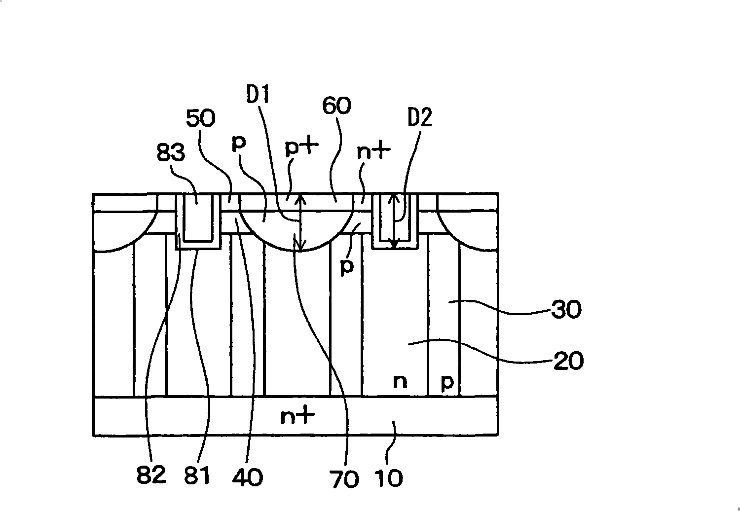
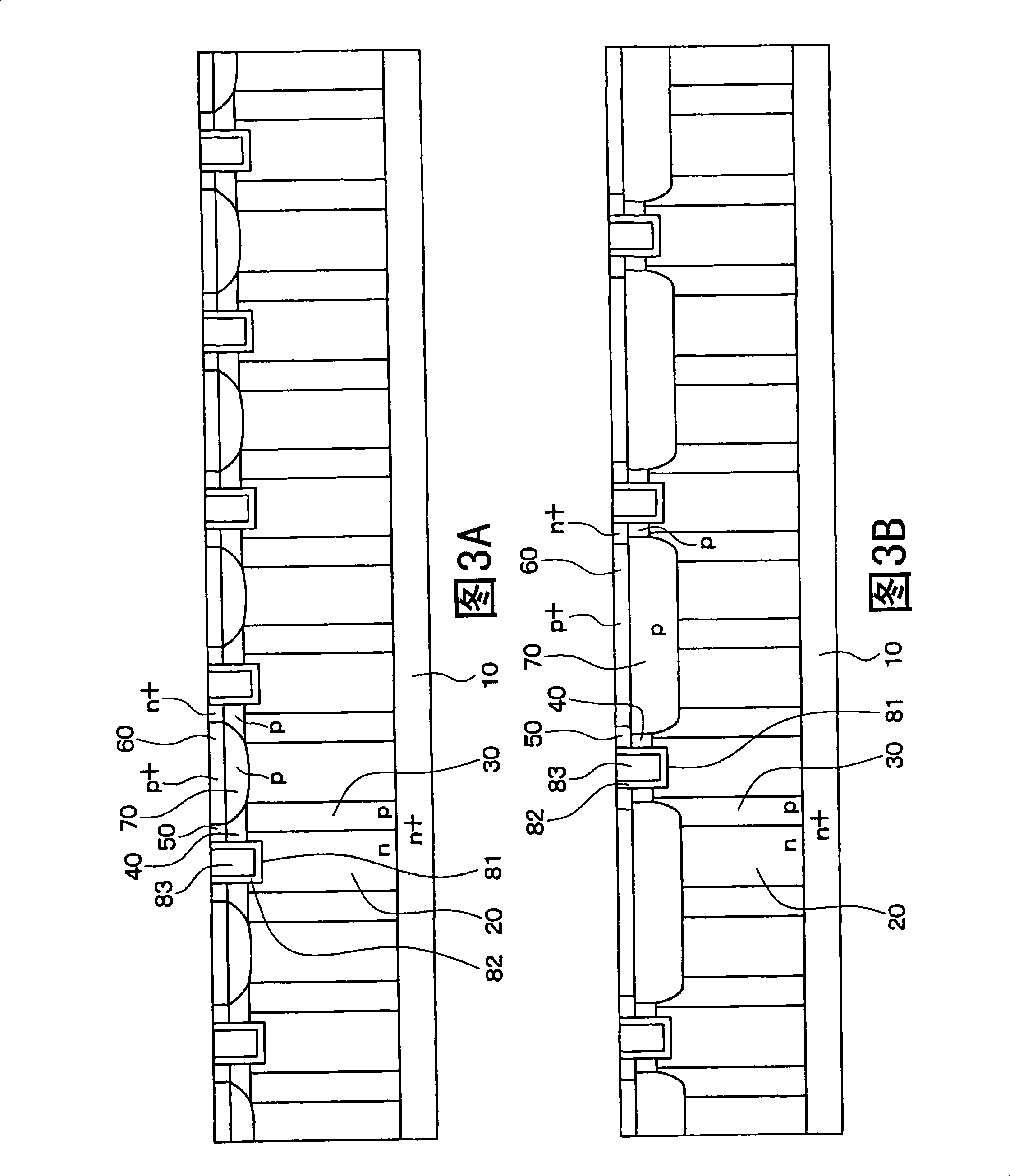
The invention relates to a semiconductor device which comprises a semiconductor substrate (10) and a super junction structure on the substrate. The super junction structure consists of p-type and n-type column regions which are alternately arranged. A p-type channel layer (40) is formed to a surface of the super junction structure. A trench gate structure is formed to the n-type column region. An n+-type source region (50) is formed to a surface of the channel layer near the trench structure. A p+-type region (60) is formed to the surface of the channel layer between adjacent n+-type source regions. A p-type body region (70) is formed in the channel layer between adjacent trench gate structures and in contact with the p+-type region. Avalanche current is caused to flow from the body region to a source electrode via the p+-type region without passing through the n+-type source region.

Description

technical field [0001] The present invention relates to a semiconductor device having a super junction structure and a trench gate type semiconductor element formed onto a semiconductor substrate. Background technique [0002] For example, as disclosed in US 6734496 corresponding to JP-A-H9-266311, a super-junction metal-oxide-semiconductor field-effect transistor (MOSFET) is proposed, which realizes an improved breakdown voltage and an improved on-resistance. In a super junction MOSFET, the drift region is formed by alternating n-type drift regions and p-type separation regions. Each p-type separation region is disposed between adjacent n-type drift regions to form a p-n junction. When the MOSFET is on, the drift current flows through the n-type drift region. Conversely, if the MOSFET is in the off state, the depletion layer extends from each p-n junction between the n-type drift region and the p-type separation region into the n-type drift region. In this case, since t...

Claims


Application Information

Patent Timeline
Patent Type & Authority Applications(China)
IPC IPC(8): H01L27/088H01L29/78H01L29/06H01L29/08H01L29/10
CPCH01L29/7813H01L29/0626H01L29/0634H01L29/1095H01L29/66734H01L29/7808H01L21/18
Inventor 柴田巧
Owner DENSO CORP
Learn More