Solid-state image pickup device and a method of manufacturing the same, and image pickup apparatus

An imaging device, a solid-state technology, applied in the field of solid-state imaging devices and its manufacturing, and imaging equipment, can solve the problems of poor color reproducibility and large influence, and achieve suppression of color reproducibility deterioration, improvement of sensitivity, and good color reproducibility Effect

Inactive Publication Date: 2008-11-19
SONY CORP
View PDF2 Cites 24 Cited by
  • Summary
  • Abstract
  • Description
  • Claims
  • Application Information

AI Technical Summary

Problems solved by technology

Therefore, if Figure 7 As shown in , the influence of the color mixture component introduced from the A pixel to its adjacent pixels is large, which causes a large influence on the adjacent pixels, such as deterioration of color reproducibility

Method used


Image

  • Solid-state image pickup device and a method of manufacturing the same, and image pickup apparatus
  • Solid-state image pickup device and a method of manufacturing the same, and image pickup apparatus
  • Solid-state image pickup device and a method of manufacturing the same, and image pickup apparatus

Examples


Embodiment Construction

[0026] Hereinafter, preferred embodiments of the present invention will be described in detail with reference to the accompanying drawings.

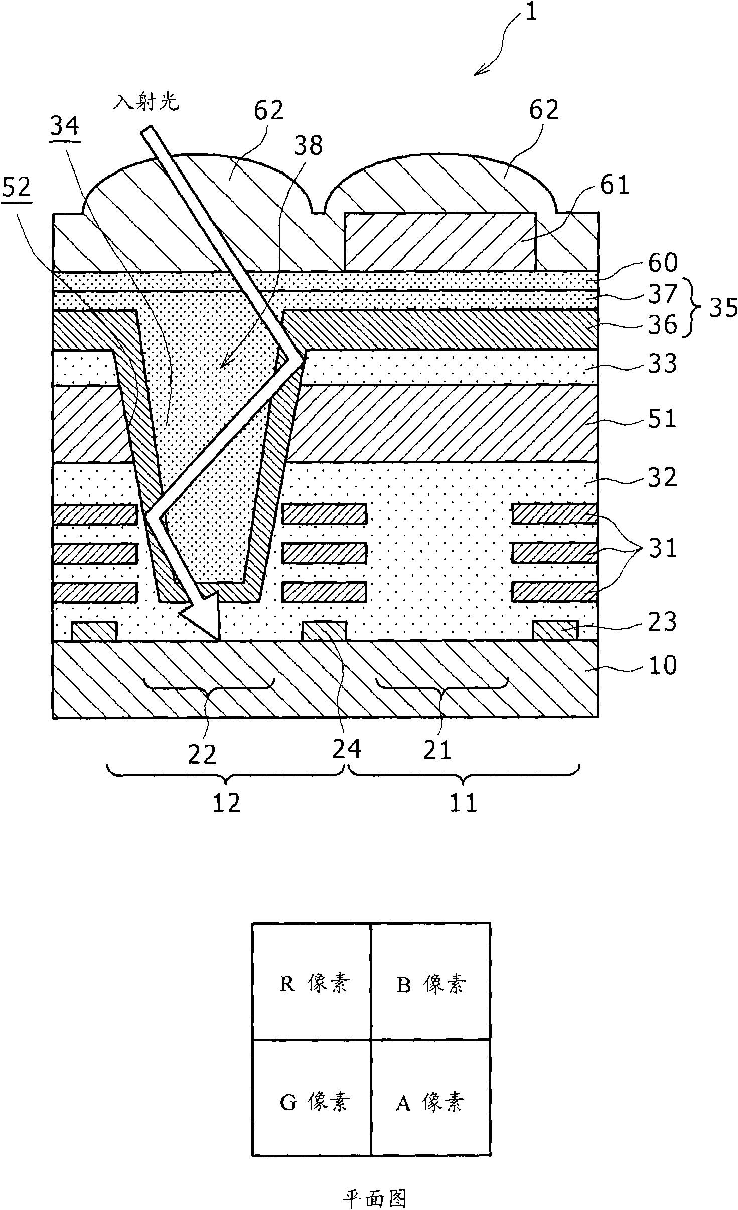
[0027] In the following, reference will be made to figure 1 A schematic structural sectional view of a solid-state imaging device according to a first embodiment of the present invention will be described in detail.

[0028] Such as figure 1 As shown, the light receiving portion 21 of the first pixel 11 (for example, composed of a photodiode), the light receiving portion 22 of the second pixel 12 (for example, composed of a photodiode), and the transistors of the first pixel 11 and the second pixel 12 23 and 24 etc. are formed on the semiconductor substrate 10 . Here, the first pixel 11 receives visible light, and the second pixel 12 receives near-infrared light and visible light. For example, if figure 1As shown on the lower side of , the first pixel 11 is composed of an R (red) pixel that receives red light, a G (green) pixel th...


PUM


Abstract

Disclosed herein is a solid-state image pickup device, including: a first pixel for receiving a visible light of an incident light to subject the visible light to photoelectric conversion; a second pixel for receiving the visible light and a near-infrared light of the incident light to subject each of the visible light and the near-infrared light to the photoelectric conversion; a color filter layer; and an infrared light filter layer for absorbing or reflecting an infrared light, and transmitting the visible light.

Description

technical field [0001] The present invention relates to a solid-state imaging device, a manufacturing method thereof, and an imaging apparatus. Background technique [0002] Currently, the infrared fitting (IR-Fitting) technology is developing towards the direction of improving the high sensitivity of the image sensor. The feature of infrared adaptation is to simultaneously extract visible light and near-infrared light in the image sensor, thereby achieving a high sensitivity improvement of the image sensor. For this reason, in addition to general RGB pixels, there are pixels (hereinafter, referred to as “A pixels”) that simultaneously extract visible light and near-infrared light in the image sensor. This technique is described, for example, in Japanese Patent Application Laid-Open No. 2006-190958 (hereinafter, referred to as Patent Document 1). [0003] In a general image sensor, an infrared light cutting filter (infrared light cutting filter) is provided over the entire...

Claims


Application Information

Patent Timeline
Patent Type & Authority Applications(China)
IPC IPC(8): H01L27/146H04N5/225H01L27/14H04N5/335H04N5/369H04N9/07H04N101/00
CPCH01L27/14636H01L27/1463H01L27/14625H04N9/045H01L27/14627H01L27/14629H01L27/14621H04N25/131H04N25/135H01L27/146H04N25/76
Inventor 井上晋
Owner SONY CORP
Why Eureka
Try Eureka