Light emitting -type optical film and process for manufacture thereof, and LCD device

A liquid crystal display device, light-emitting technology, applied in optics, nonlinear optics, instruments, etc., can solve the problems of low light use efficiency, complicated process, high material cost, etc., and achieve the effect of increasing light-emitting function and reducing cost

Inactive Publication Date: 2008-11-26
台湾薄膜电晶体液晶显示器产业协会 +6
View PDF0 Cites 5 Cited by
  • Summary
  • Abstract
  • Description
  • Claims
  • Application Information

AI Technical Summary

Problems solved by technology

[0002] For the traditional optical film process and design used in displays, the process is not only complicated and costly, but also requires the support or protection of the substrate layer to complete the production and design of the optical film. Limit materials and functions; too many substrates not only lead to high material costs, but also directly or indirectly have a great impact on optical properties, and also cause high thickness of optical films
[0003] In addition, since the liquid crystal panel is a non-self-illuminating display panel, the current liquid crystal display device needs a backlight module to provide a backlight source. In addition, the light use efficiency is low. To achieve high image quality, high brightness, low power consumption or high Fine characteristics require a variety of optical films to improve or enhance its optical properties, such as polarizing film, wide viewing angle film, diffusion film, prism film (also known as brightness enhancement film), etc.

Method used


Image

  • Light emitting -type optical film and process for manufacture thereof,  and LCD device
  • Light emitting -type optical film and process for manufacture thereof,  and LCD device
  • Light emitting -type optical film and process for manufacture thereof,  and LCD device

Examples


no. 1 example

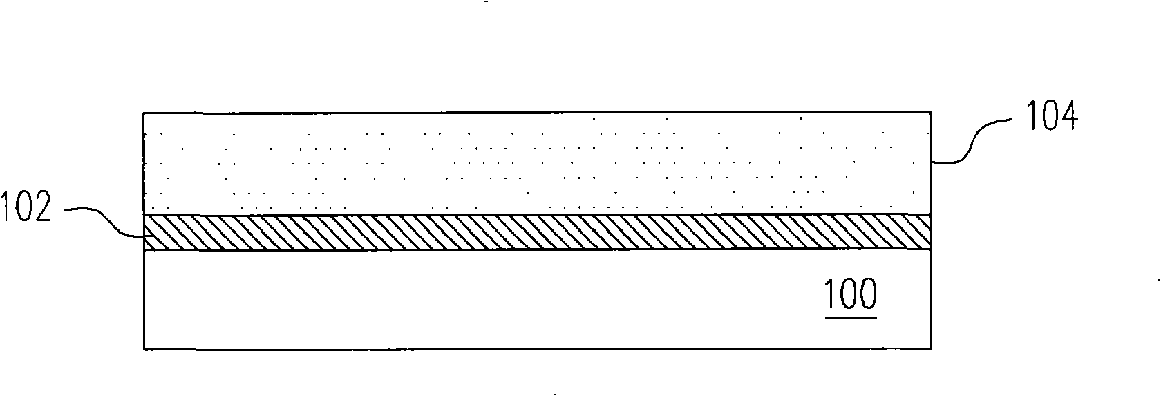
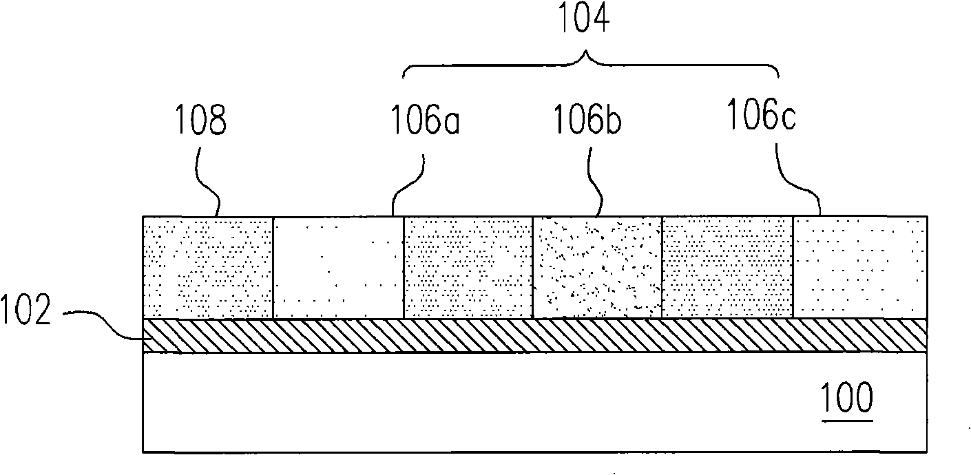
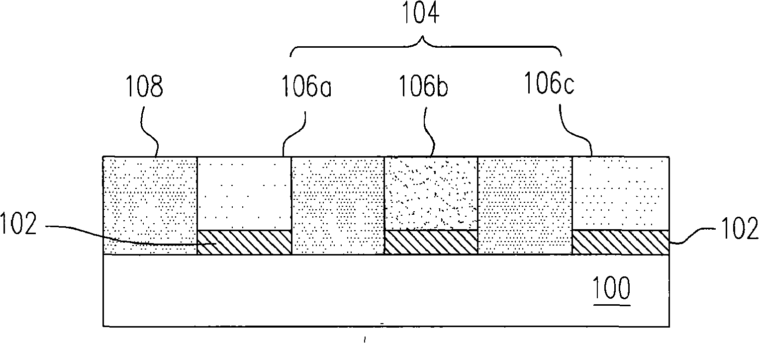
[0052] Figure 1A to Figure 1C They are respectively structural cross-sectional views of three variations of the light-emitting optical film according to the first embodiment of the present invention.

[0053] Please refer to Figure 1A , the first light-emitting optical film is composed of a substrate 100, an alignment layer 102, and a layer of polarized liquid crystal film 104, wherein the polarized liquid crystal film 104 includes liquid crystals and light-emitting dyes, and the type of liquid crystal For example, polymer liquid crystal (liquid crystal polymer), oligomer liquid crystal (liquid crystal oligomer) or liquid crystal monomer (monomer); light-emitting dyes are organic light-emitting diodes (organic light- emitting diode, OLED) dye. Moreover, the light-emitting liquid crystal film 104 can change its luminescent color according to the characteristic that different light-emitting dyes have different wavelengths. As for the substrate 100, it may be a transparent su...

no. 2 example

[0058] figure 2 It is a process step diagram of a light-emitting optical film according to the second embodiment of the present invention.

[0059] Please refer to figure 2 , in step 200, a substrate is provided, and the substrate is a light-transmitting substrate or an opaque substrate. Also, there is an alignment layer on one side of the substrate.

[0060] Then, in step 102, a layer of polarized liquid crystal film is formed on the alignment layer by coating, wherein the polarized liquid crystal film is at least composed of liquid crystal and luminescent dye. The raw material of the above-mentioned polarizing liquid crystal film is to dissolve luminescent dyes in liquid crystals, and combine the absorption and light emission of different luminescent dyes with liquid crystals to apply to polarizing films that emit polarized light or compensation films that emit polarized light. Functional optical film. In addition, in addition to coating the liquid crystal containing l...

no. 3 example

[0066] The liquid crystal display device of the third embodiment mainly includes a liquid crystal panel and a light emitting source. Moreover, the liquid crystal panel includes at least one component, which is composed of a layer of second alignment layer and a layer of polarized liquid crystal film, wherein the polarized liquid crystal film includes liquid crystal and luminescent dye. As for the light emitting source, it is located on either side of the liquid crystal panel, and the light emitted by the light emitting source can make the polarized liquid crystal film emit light in a different wavelength range. The following is an exploded view of several structural sections.

[0067] Please refer to Figure 6A , the liquid crystal display device of this embodiment includes a liquid crystal panel 600 a and a light source 602 . The liquid crystal panel 600 a includes two electrode substrates 604 , a liquid crystal layer 606 between the electrode substrates 604 , and two first...


PUM


Abstract

The invention discloses a luminous optical film, a manufacturing method of the luminous optical film and a liquid crystal display device. The luminous optical film at least is composed of a base material, an alignment layer and a layer of polarized liquid crystal film, wherein, the polarized liquid crystal film comprises liquid crystal and luminous dyestuffs. The alignment layer is arranged at one side of the base material. The polarized liquid crystal film is arranged above the alignment layer. The luminous optical film can be applicable to a polarized film, a compensation film or a color filter. The luminous optical film can give out uniform polarized light owning to the overall arrangement of the liquid crystal. Therefore, a conventional backlight module is not required, thus greatly reducing expenses on the conventional backlight module.

Description

technical field [0001] The present invention relates to an optical film structure and a manufacturing method thereof, and in particular to a light emitting optical film, a manufacturing method thereof and a liquid crystal display device. Background technique [0002] For the traditional optical film process and design used in displays, the process is not only complicated and costly, but also requires the support or protection of the substrate layer to complete the production and design of the optical film. Limit materials and functions; too many substrates not only lead to high material costs, but also directly or indirectly have a great impact on optical properties, and also cause high thickness of optical films. [0003] In addition, since the liquid crystal panel is a non-self-illuminating display panel, the current liquid crystal display device needs a backlight module to provide a backlight source. In addition, the light use efficiency is low. To achieve high image qual...

Claims


Application Information

Patent Timeline
Patent Type & Authority Applications(China)
IPC IPC(8): G02F1/13G02F1/1333G02F1/1335
Inventor 郑岳世杨界雄
Owner 台湾薄膜电晶体液晶显示器产业协会
Why Eureka
Try Eureka