Method for forming amorphous carbon film and method for manufacturing semiconductor device using the method

An amorphous carbon film and semiconductor technology, which is applied in semiconductor/solid-state device manufacturing, photosensitive materials for optomechanical equipment, gaseous chemical plating, etc., can solve high cost, poor quality of amorphous carbon film, and long processing time. Time and other issues

Inactive Publication Date: 2008-11-26
TES CO LTD
View PDF0 Cites 15 Cited by
  • Summary
  • Abstract
  • Description
  • Claims
  • Application Information

AI Technical Summary

Problems solved by technology

Because reaction by-products often adhere to the inner walls of the chamber, the cleaning process should be performed more frequently, which results in longer processing times and higher costs
At the same time, reaction by-products are not easily removed from the chamber during cleaning
Thus, the quality of the amorphous carbon film deteriorates, and the part replacement cycle of the chamber is shortened

Method used


Image

  • Method for forming amorphous carbon film and method for manufacturing semiconductor device using the method
  • Method for forming amorphous carbon film and method for manufacturing semiconductor device using the method
  • Method for forming amorphous carbon film and method for manufacturing semiconductor device using the method

Examples


no. 1 example

[0063] First Example: Characterization of Amorphous Carbon Films as a Function of RF Power

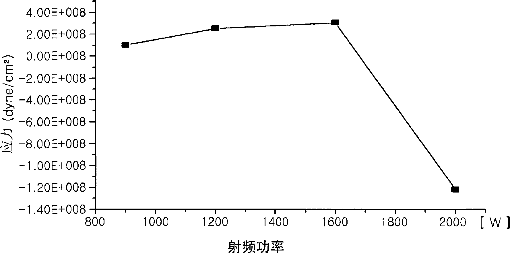
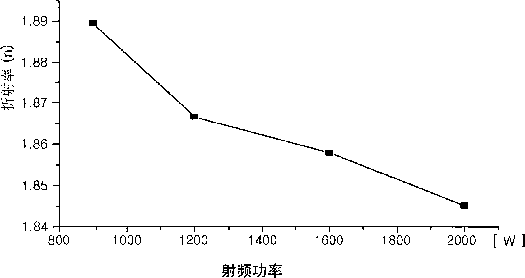
[0064] In the first example of the present invention, hexene was supplied at a flow rate of 0.8 g / min (C 6 h 12 ), argon gas was supplied at a flow rate of 300 sccm and helium gas was supplied at a flow rate of 800 sccm to form an amorphous carbon film. Additionally, a distance of 350 mils was maintained between the showerhead and the substrate. Figures 2A to 2D The changes of stress, refractive index (n), light absorption coefficient (k) and deposition rate of amorphous carbon film according to RF power are illustrated respectively.

[0065] Figure 2A It is a graph illustrating the change of the stress of the amorphous carbon film according to the RF power. see Figure 2A , as the RF power increased, the stress increased slightly and then decreased significantly after the RF power became 1600W.

[0066] Figure 2B is a graph illustrating the change in the refractive index (n)...

no. 2 example

[0071] Second example: change of characteristics of amorphous carbon film depending on the amount of reaction source to be supplied

[0072] In a second example of the present invention, hexene (C 6 h 12 ), argon gas was supplied at a flow rate of 300 sccm and helium gas was supplied at a flow rate of 200 sccm to form an amorphous carbon film. Additionally, a distance of 320 mils was maintained between the showerhead and the substrate. In this situation, Figures 3A to 3D Changes in the stress, refractive index (n), light absorption coefficient (k) and deposition rate of the amorphous carbon film depending on the amount of the reaction source to be supplied are described respectively.

[0073] Figure 3A is a graph illustrating that the stress of the amorphous carbon film changes depending on the amount of the reaction source to be supplied. see Figure 3A , as the amount of reactive source to be supplied increases, the stress decreases.

[0074] Figure 3B is a graph ...

no. 3 example

[0079] Example 3: Characteristics of an amorphous carbon film depending on the distance between the shower head and the substrate

[0080] In a third example of the present invention, hexene (C 6 h 12 ), argon gas was supplied at a flow rate of 300 sccm and helium gas was supplied at a flow rate of 800 sccm to form an amorphous carbon film. Additionally, the distance between the showerhead and the substrate was varied in the range of 250 to 350 mils. In this situation, Figures 4A to 4D The variation of stress, refractive index (n), light absorption coefficient (k) and deposition rate of amorphous carbon film according to the distance between the shower head and the substrate are illustrated respectively.

[0081] Figure 4A is a graph illustrating how the stress of an amorphous carbon film varies depending on the distance between the shower head and the substrate. see Figure 4A , as the distance between the showerhead and the substrate becomes larger, the stress decrea...


PUM

PropertyMeasurementUnit
refractive indexaaaaaaaaaa

Abstract

The present invention relates to a method of forming an amorphous carbon film and a method of manufacturing a semiconductor device using the method. An amorphous carbon film is formed on a substrate by vaporizing a liquid hydrocarbon compound, which has chain structure and one double bond, and supplying the compound to a chamber, and ionizing the compound. The amorphous carbon film is used as a hard mask film. It is possible to easily control characteristics of the amorphous carbon film, such as a deposition rate, an etching selectivity, a refractive index (n), a light absorption coefficient (k) and stress, so as to satisfy user's requirements. In particular, it is possible to lower the refractive index (n) and the light absorption coefficient (k). As a result, it is possible to perform a photolithography process without an antireflection film that prevents the diffuse reflection of a lower material layer. Further, a small amount of reaction by-product is generated during a deposition process, and it is possible to easily remove reaction by-products that are attached on the inner wall of a chamber. For this reason, it is possible to increase a cycle of a process for cleaning a chamber, and to increase parts changing cycles of a chamber. As a result, it is possible to save time and cost.

Description

technical field [0001] The present invention relates to a method of forming an amorphous carbon film, and more particularly, to a method of forming an amorphous carbon film having a low light absorption coefficient and a wide range of refractive index by using a liquid hydrocarbon and a A method of manufacturing a semiconductor device using the method. Background technique [0002] A semiconductor device includes various elements, such as word lines, bit lines, capacitors, and metal lines, which interact with each other. As the degree of integration and performance of semiconductor devices increases, demands on materials and process technologies for manufacturing semiconductor devices also increase. Specifically, the increase in integration is accompanied by the reduction in size of semiconductor devices, and methods for forming fine patterns for various structures on semiconductor substrates have been continuously studied. [0003] Due to the increasing need for improved ...

Claims


Application Information

Patent Timeline
Patent Type & Authority Applications(China)
IPC IPC(8): H01L21/033C23C16/26C23C16/44
CPCH01L21/3146C23C16/26G03F7/11H01L21/02527H01L21/02592H01L21/0262H01L21/0276H01L21/0332H01L21/02115H01L21/205
Inventor 朴根五安秉大李承俊
Owner TES CO LTD
Why Eureka
Try Eureka