

NMOS transistor and method for forming same
A transistor and pocket-shaped technology, applied in the field of NMOS transistors and their formation, can solve problems such as the influence of undisclosed NMOS transistor performance, and achieve the effect of improving the driving current capability
- Summary
- Abstract
- Description
- Claims
- Application Information
AI Technical Summary
Problems solved by technology
Method used
Image

Examples
Embodiment Construction
[0026] The invention provides an NMOS transistor and a forming method thereof, which increase the drive current of the NMOS transistor and reduce the leakage current while keeping the threshold voltage unchanged from the prior art.
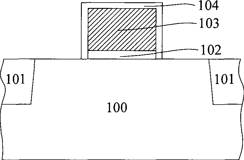
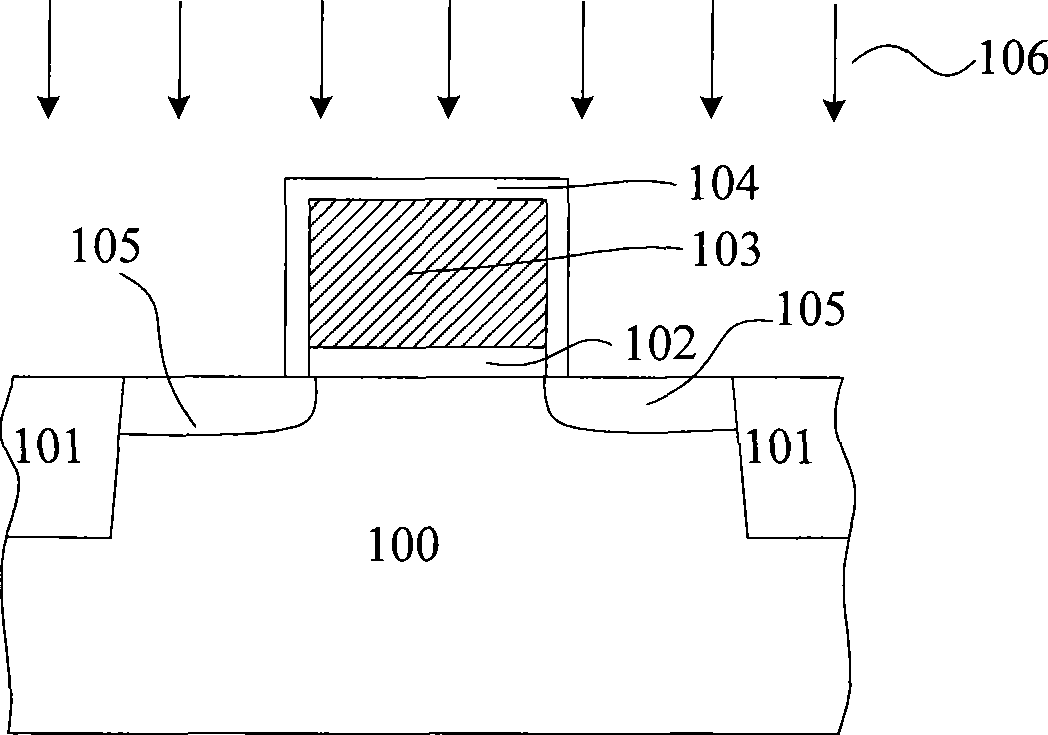
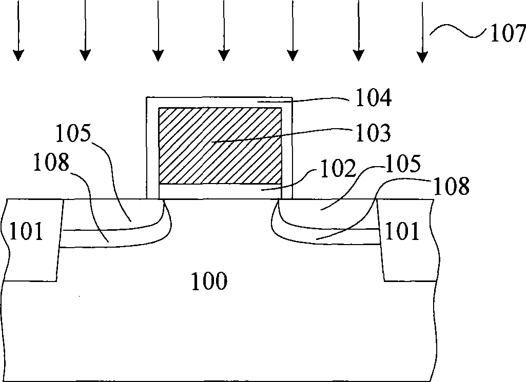
[0027] First, the present invention provides a method for forming an NMOS transistor, comprising the following steps: sequentially forming a gate dielectric layer and a polysilicon gate on a semiconductor substrate, the gate dielectric layer and the polysilicon gate forming a gate structure; Implant carbon ions into the semiconductor substrate to form carbon ion doped regions; form source / drain extension regions on both sides of the gate structure and in the semiconductor substrate; form source / drain electrodes on both sides of the gate structure and in the semiconductor substrate , the depth of the carbon ion doped region is bounded between the surface of the semiconductor substrate and the source / drain; the semiconductor substrate is annealed to ...
PUM
 Abstract
Description
Claims
Application Information