Semiconductor interposer and its application in electronic package

一种半导体、中介的技术,应用在标准可编程中介片领域,能够解决不便、一般产品及方法没有适切结构及方法等问题,达到减低成本与周期时间、缩减周期时间的效果

Active Publication Date: 2008-12-03
TAIWAN SEMICON MFG CO LTD
View PDF0 Cites 36 Cited by
  • Summary
  • Abstract
  • Description
  • Claims
  • Application Information

AI Technical Summary

Problems solved by technology

[0006] It can be seen that the above-mentioned existing semiconductor interposer and its application in electronic packaging obviously still have inconvenience and defects in product structure, manufacturing method and use, and need to be further improved urgently.
In order to solve the above-mentioned existing problems, relevant manufacturers have tried their best to find a solution, but for a long time no suitable design has been developed, and general products and methods do not have appropriate structures and methods to solve the above-mentioned problems. This is obviously a problem that relevant industry players are eager to solve

Method used


Image

  • Semiconductor interposer and its application in electronic package
  • Semiconductor interposer and its application in electronic package
  • Semiconductor interposer and its application in electronic package

Examples


Embodiment Construction

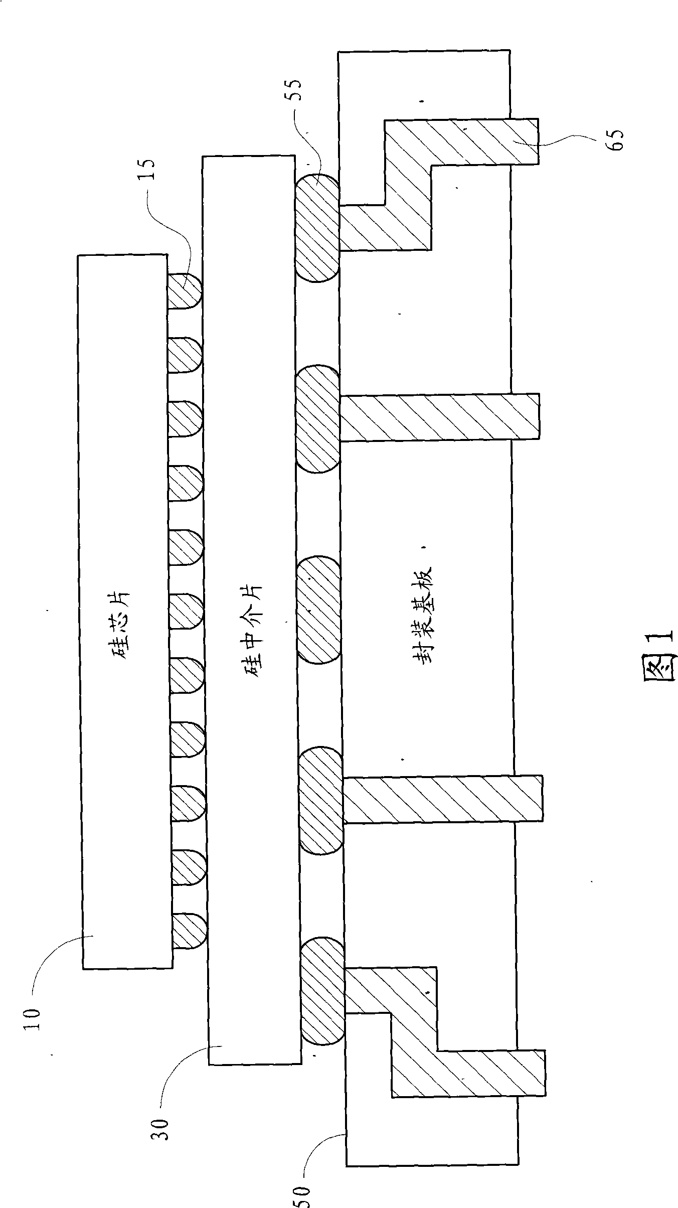
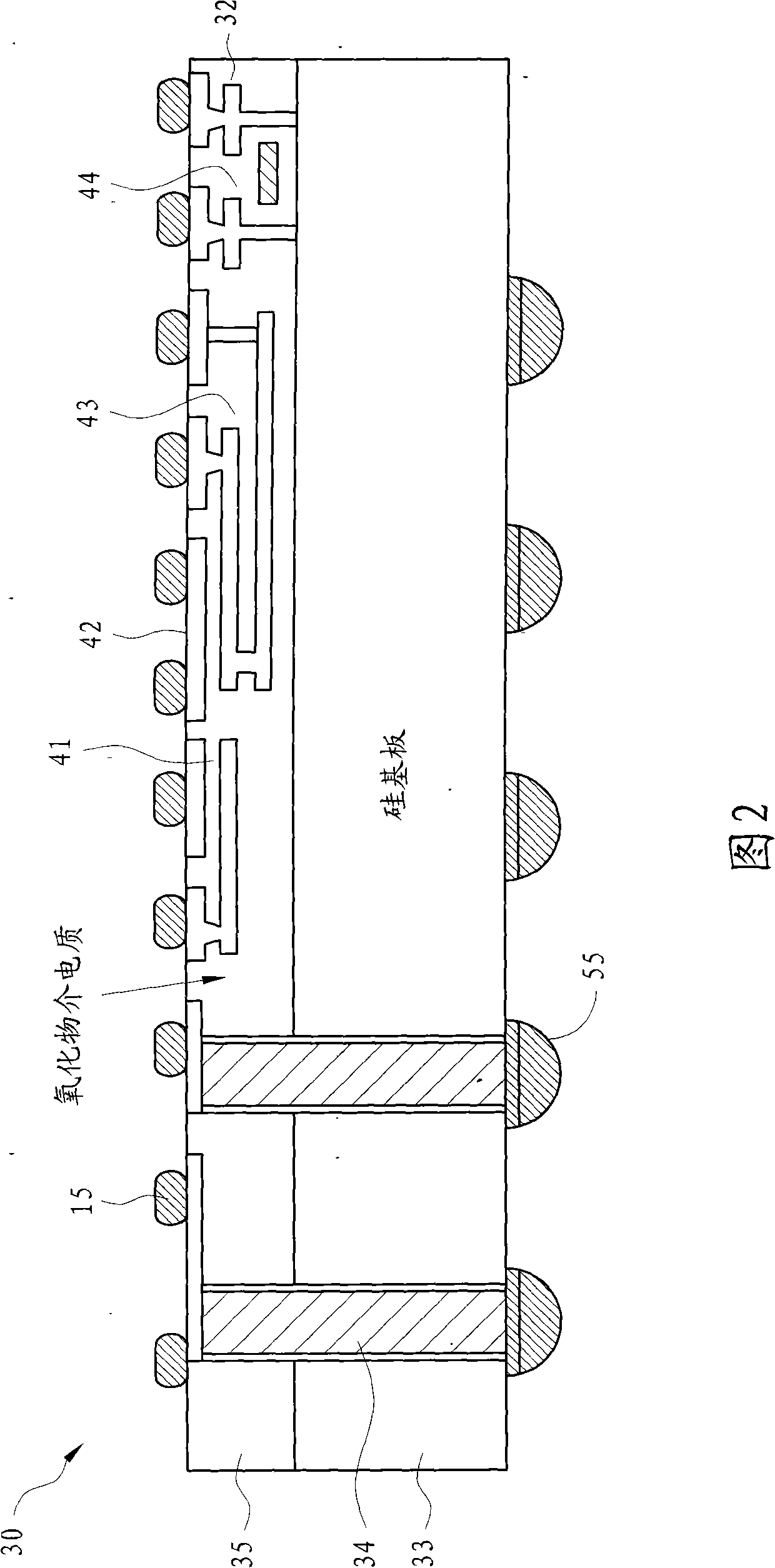
[0111] In order to further explain the technical means and effects of the present invention to achieve the intended purpose of the invention, the specific implementation of the semiconductor interposer proposed according to the present invention and its application in electronic packaging will be described below in conjunction with the accompanying drawings and preferred embodiments. , structure, method, step, feature and effect thereof, detailed description is as follows.

[0112] The present invention will be described in terms of preferred embodiments in the specific context of a standardized, user-programmable silicon interposer structure and method of fabrication thereof, wherein the standardized, user-programmable silicon interposer The structure has several passive and / or active elements arranged in an array. The invention also includes the structure of the electronic package including at least the interposer and its manufacturing method.

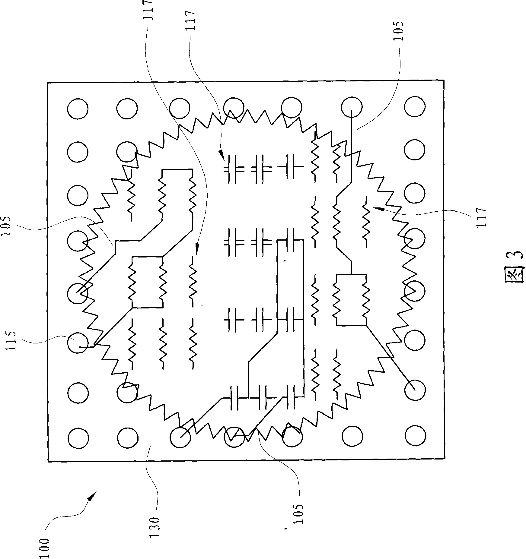
[0113] FIG. 3 is a schematic...


PUM


Abstract

Various structures of a programmable semiconductor interposer for electronic packaging are described. An array of semiconductor devices having various values is formed in said interposer. A user can program said interposer and form a ''virtual'' device having a desired value by selectively connecting various one of the array of devices to contact pads formed on the surface of said interposer. An inventive electronic package structure includes a standard interposer having an array of unconnected devices of various values and a device selection unit, which selectively connects various one of the array of devices in said standard interposer to an integrated circuit die encapsulated in said electronic package. Methods of forming said programmable semiconductor interposer and said electronic package are also illustrated.

Description

technical field [0001] The present invention relates to a kind of semiconductor interposer (Interposer) of electronic package and its manufacturing method, particularly relate to a kind of standard programmable interposer, the required circuit function is formed in this programmable interposer, and these circuit functions are coupled to the integrated circuit chip attached to the interposer. Background technique [0002] As the trend to provide substantially increased circuit functionality on integrated circuits continues, so-called System-On-Chip (SOC) integrated circuit architectures are rapidly gaining popularity in almost all application areas of integrated circuits. Therefore, it has been necessary to form a very large number of transistors on an integrated circuit chip. At the same time, forming complex electronic systems on an integrated circuit chip requires a large number of input / output (I / O) contacts between the integrated circuit chip and the rest of the electro...

Claims


Application Information

Patent Timeline
Patent Type & Authority Applications(China)
IPC IPC(8): H01L23/48
CPCH01L23/5382H01L23/49827H01L2924/15174H01L21/76886H01L2224/16H01L23/147H01L2924/13091H01L2924/15192H01L2924/19011H01L2924/15311H01L23/642H01L2924/01078H01L2924/10253H01L23/645H01L2924/1461H01L2924/1305H01L2924/00014H01L25/0652H01L25/0655H01L25/0657H01L2224/13025H01L2224/16145H01L2224/16146H01L2224/16227H01L2224/16235H01L2224/17181H01L2225/06517H01L2225/06589H01L2924/157H01L2225/06513H01L2225/06541H01L2924/00011H01L2224/16225H01L2924/00H01L2224/0401
Inventor 许昭顺赵智杰彭迈杉
Owner TAIWAN SEMICON MFG CO LTD
Why Eureka
Try Eureka