Insulated gate bipolar transistor

A technology of bipolar transistors and insulated gates, which is applied in the manufacture of transistors, semiconductor devices, semiconductor/solid-state devices, etc., and can solve the problems of easily weakened conductivity modulation

Inactive Publication Date: 2008-12-17
SANYO ELECTRIC CO LTD +1
View PDF1 Cites 10 Cited by
  • Summary
  • Abstract
  • Description
  • Claims
  • Application Information

AI Technical Summary

Problems solved by technology

Therefore, the influence of the detachment of holes from the emitter electrode 78 in contact between the trenches 72 is large, and the conductivity modulation tends to be weakened.

Method used


Image

  • Insulated gate bipolar transistor
  • Insulated gate bipolar transistor
  • Insulated gate bipolar transistor

Examples


Embodiment Construction

[0030] Hereinafter, embodiments of the insulated gate bipolar transistor according to the present invention will be described in detail with reference to the drawings.

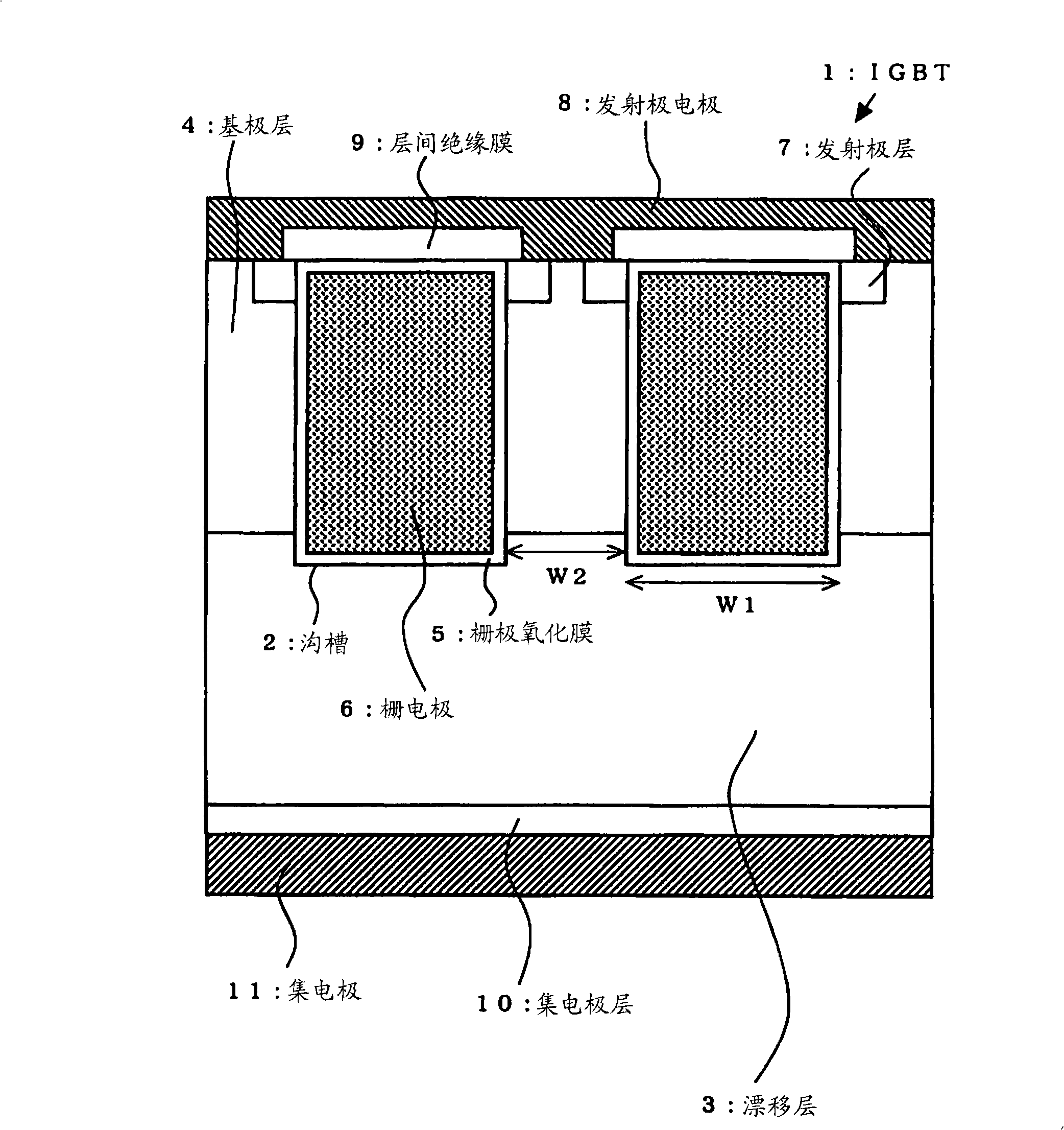
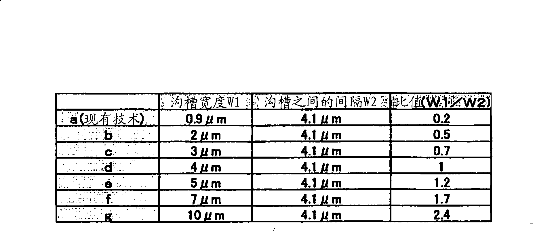
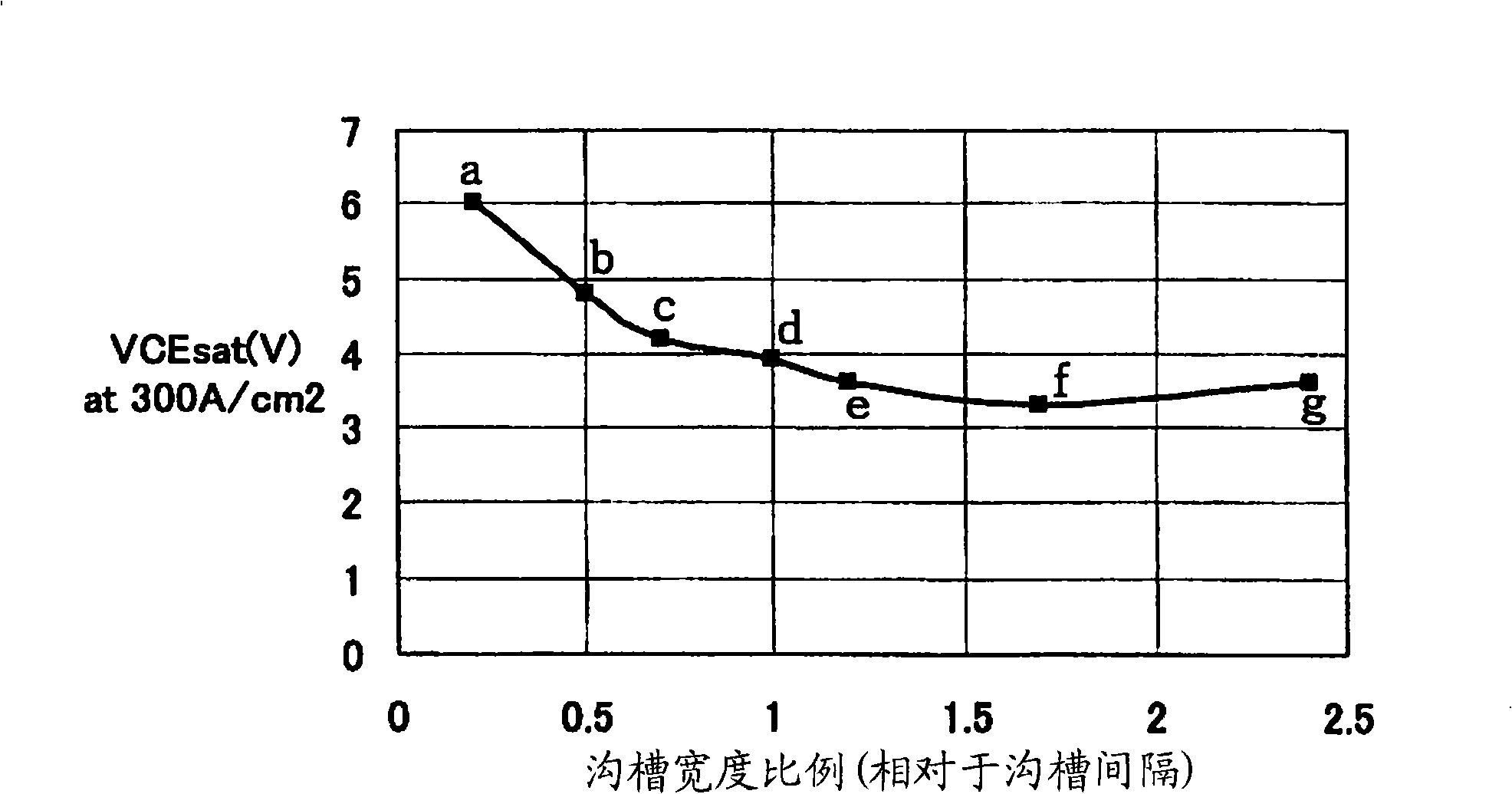
[0031] figure 1 A cross-sectional view showing a trench-type IGBT 1 having an NPT structure according to the present embodiment. In addition, in this figure, the grooves 2 are formed at only two positions for simplicity, but actually, a plurality of grooves are formed in stripes at predetermined intervals in a plan view.

[0032] The IGBT 1 has: an N-drift layer 3 composed of an FZ wafer; a P-type base layer 4 formed on the main surface of the drift layer 3; a plurality of trenches 2 formed by Formed to reach the drift layer 3 from the surface of the base layer 4; an insulating gate, which is formed in the trench 2 through a gate oxide film 5 to form a gate electrode 6; an N+ type emitter layer 7, which is formed in The main surface of the base layer 4 is adjacent to the insulating gate; the emitter electro...


PUM


Abstract

The invention realizes IGBT having an NPT structure which has a smaller variation in switching characteristics and the like and lower on-resistance. In the IGBT of the invention, by setting a ratio of a width of a trench to an interval between the trenches within a range of 1 to 2, electron current density and a conductivity modulation effect are optimized, a breakdown voltage is secured, a variation in characteristics is minimized, and on-resistance is largely reduced.

Description

technical field [0001] The invention relates to an insulated gate bipolar transistor, in particular to an insulated gate bipolar transistor with a trench structure. Background technique [0002] The insulated gate bipolar transistor is called IGBT (Insulated-Gate Bipolar Transistor), and has become one of the mainstreams of high-current switches. [0003] Figure 7 (a) shows a cross-sectional view of a trench-type IGBT having a punch-through (Punch Through, PT) structure according to the prior art. [0004] In the IGBT 51 having a PT structure, an N-type buffer layer 62 and an N-type drift layer 53 are epitaxially grown sequentially on a collector layer 60 formed of a P+ type semiconductor substrate. Furthermore, a P-type base layer 54 is formed on the main surface of the drift layer 53 , and a plurality of trenches 52 are formed so as to reach the drift layer 53 from the surface of the base layer 54 . In this figure, the grooves 52 are formed at only two positions for sim...

Claims


Application Information

Patent Timeline
Patent Type & Authority Applications(China)
IPC IPC(8): H01L29/739H01L29/06
CPCH01L29/66348H01L29/7397H01L29/73H01L21/18
Inventor 冈田喜久雄
Owner SANYO ELECTRIC CO LTD
Why Eureka
Try Eureka