Technique for thinning back side of silicon wafer

A backside thinning and wafer technology, used in manufacturing tools, metal processing equipment, machine tools with surface polishing, etc., can solve the problems of wafer edge bending and fracture, and achieve the effect of improving quality

Active Publication Date: 2008-12-24
SEMICON MFG INT (SHANGHAI) CORP +1
View PDF1 Cites 22 Cited by
  • Summary
  • Abstract
  • Description
  • Claims
  • Application Information

AI Technical Summary

Problems solved by technology

[0005] The present invention aims to solve the problem that the edge of the wafer is easily bent or even broken when thinning the back of the wafer in the prior art

Method used


Image

  • Technique for thinning back side of silicon wafer
  • Technique for thinning back side of silicon wafer
  • Technique for thinning back side of silicon wafer

Examples


Embodiment 1

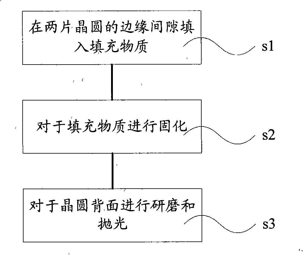
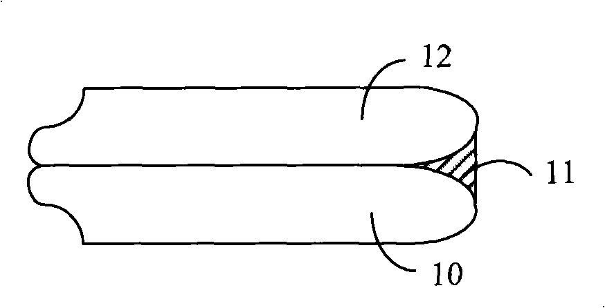
[0020] combine figure 2 and Figure 3A As shown, before wafer 10 and wafer 12 backsides are thinned, the bonded wafer 10 and wafer 12 are first erected by a robotic arm, and then filled with a filling material 11, such as silica gel, by a dispenser. Insert the gap between the circumferential edges of the two wafers, and while filling the silica gel, slowly rotate the two wafers so that the silica gel is evenly filled into the edge gap of the two wafers. Moreover, the thickness of the filled silica gel is 0.5-2mm, such as 0.5mm or 2mm or 1mm. Of course, the filling substance 11 is not limited to silica gel, and can also be other substances that do not react with the grinding slurry.

[0021] combine figure 2 and Figure 3B As shown, after the filling of the filling substance 11 is completed, the filling substance 11 needs to be cured to increase the hardness of the filling substance 11 . A commonly used curing method is to bake the filling substance 11. The curing proces...


PUM


Abstract

The present invention discloses a wafer back-thinning technique. A filling substance is filled in the gap between the edges of two wafers or the gap between the edges of a wafer and a supporting carrier; then the back of the wafer is ground, so that the thickness of the wafer can be reduced; finally, after grinding, the back of the wafer is polished. The wafer back-thinning technique of the present invention ensures that the edge of the wafer cannot be curved or broken, thus increasing the wafer-thinning quality.

Description

technical field [0001] The invention relates to a three-dimensional packaging process, in particular to a wafer back thinning process in the three-dimensional packaging process. Background technique [0002] As we all know, packaging technology is actually a technology for packaging chips, which is necessary for chips. Because the chip must be isolated from the outside world to prevent impurities in the air from corroding the chip circuit and causing electrical performance degradation. On the other hand, packaged chips are also easier to install and transport. Since the quality of the packaging technology also directly affects the performance of the chip itself and the design and manufacture of the PCB (printed circuit board) connected to it, it is very important. Packaging can also be said to be a shell for installing semiconductor integrated circuit chips. It not only plays the role of placing, fixing, sealing, protecting chips and enhancing thermal conductivity, but als...

Claims


Application Information

Patent Timeline
Patent Type & Authority Applications(China)
IPC IPC(8): B24B37/04B24B29/00H01L21/304B24B37/02
Inventor 黄河陈建华高大为毛剑宏
Owner SEMICON MFG INT (SHANGHAI) CORP
Why Eureka
Try Eureka