Encapsulation construction and encapsulation method

A packaging structure and packaging method technology, applied in the direction of electrical components, electrical solid devices, circuits, etc., can solve the problems of increasing process complexity and time, increasing the difficulty of conductive shells, and falling off of electric shells, so as to save substrate materials , Save packaging time and simplify the packaging process

Active Publication Date: 2009-01-07
ADVANCED SEMICON ENG INC
View PDF0 Cites 16 Cited by
  • Summary
  • Abstract
  • Description
  • Claims
  • Application Information

AI Technical Summary

Problems solved by technology

However, this method of fixing the conductive shell with glue, in addition to increasing the complexity and time of the manufacturing process, is prone to the problem of the conductive shell falling off due to changes in the properties of the glue due to temperature and humidity.
In addition, the size of the conductive shell and the package must match, and packages of different sizes must be made with different shells, which increases the difficulty of manufacturing the conductive shell

Method used


Image

  • Encapsulation construction and encapsulation method
  • Encapsulation construction and encapsulation method
  • Encapsulation construction and encapsulation method

Examples


Embodiment Construction

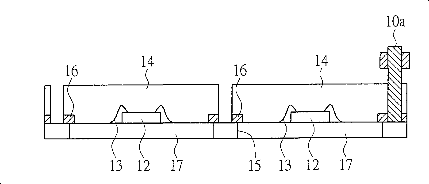
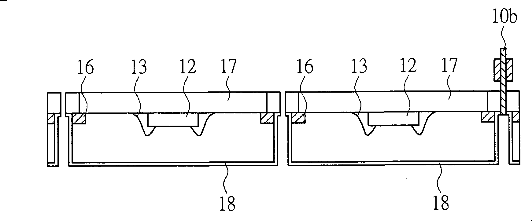
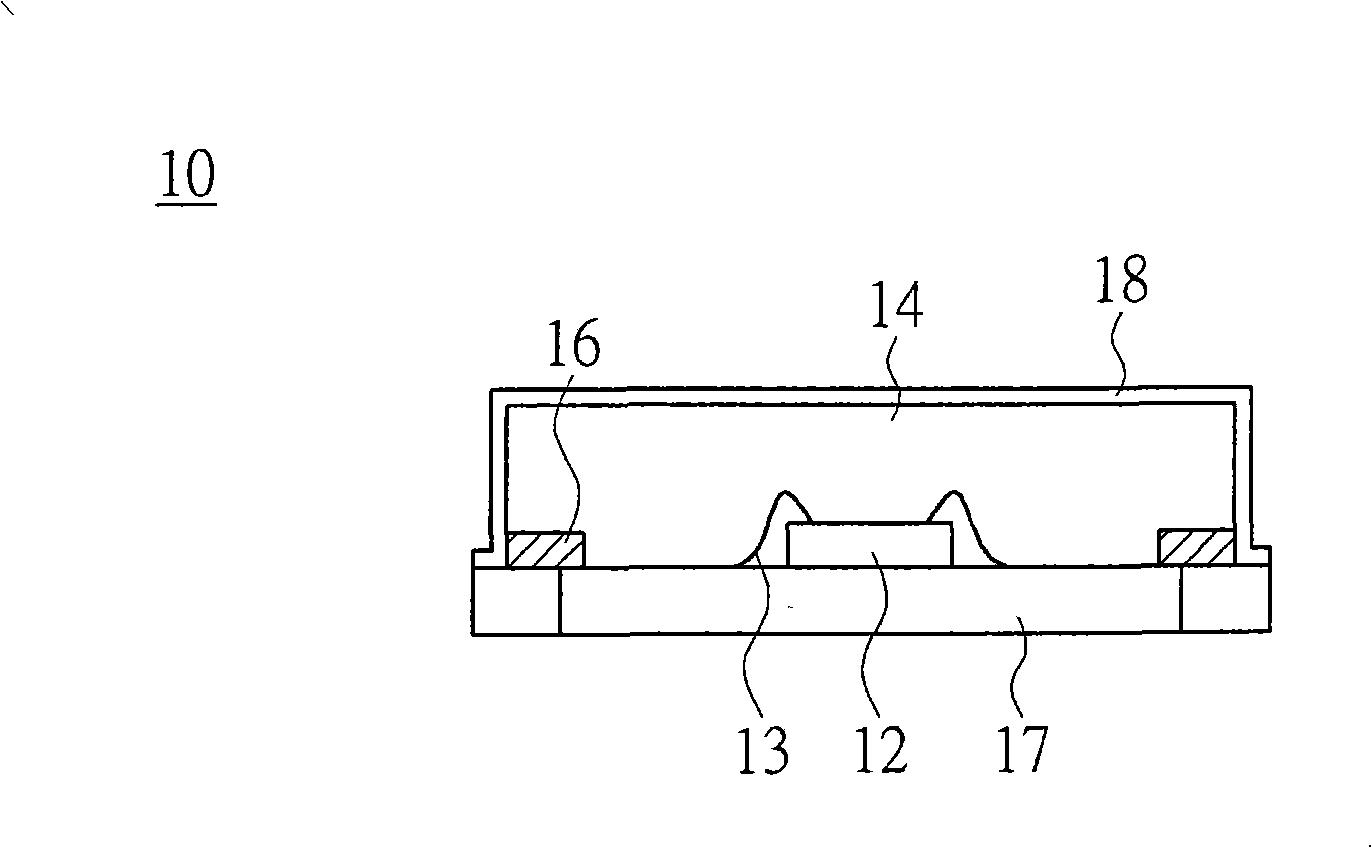
[0019] The invention proposes a packaging structure, which includes a substrate, a semiconductor component, sealing colloid and a conductive film. The substrate has a first surface, a second surface, a first side and a ground component, and the first side connects the first surface and the second surface. The semiconductor component is disposed on the first surface and electrically connected with the substrate. The ground component is disposed inside the substrate and exposed on the first side surface, and has a plane. The encapsulant covers the semiconductor component, and a second side surface of the encapsulant is substantially aligned with the plane of the grounding component. The conductive film is directly formed on an outer surface of the encapsulant, the exposed plane of the grounding component and the side of the substrate, and the conductive film is electrically connected to the grounding component. Hereby give examples and describe as follows.

[0020] Please ref...


PUM


Abstract

A package structure comprises a substrate, a semiconductor assembly, a sealing glue and a conductive film. The substrate possesses a first surface, a second surface, a first side surface and an earthing assembly. The first side surface connects first surface and second surface. The earthing assembly is disposed inside of substrate and exposed at the first side surface and possesses a plane. The semiconductor assembly is disposed at the first surface and electrically connected with substrate. The sealing glue is covered on semiconductor assembly; a second side surface of sealing glue is trimming with plane. The conductive film directly forms on one external surface of sealing glue, exposed plane of earthing assembly and the first side surface of substrate; the conductive film is electrically connected with earthing assembly.

Description

【Technical field】 [0001] The present invention relates to a package structure and a package method thereof, and in particular to an anti-electromagnetic interference package structure and a package method thereof. 【Background technique】 [0002] In general, semiconductor device packaging is to place circuits on circuit substrates, such as printed circuit boards or ceramic substrates. The performance of its circuits may be adversely affected by electromagnetic interference (EMI). Electromagnetic Interference (EMI) is signal interference or noise due to the emission of energy from electromagnetic fields. As the density of electronic components in the system is getting higher and higher, the related operating frequency is also developing to a higher frequency band, so unnecessary radiated noise becomes more obvious, which in turn leads to more serious electromagnetic interference. Therefore, various packaging structures for preventing electromagnetic interference using conduc...

Claims


Application Information

Patent Timeline
Patent Type & Authority Applications(China)
IPC IPC(8): H01L23/552H01L23/31H01L23/488H01L21/50H01L21/56H01L21/60
CPCH01L24/97H01L2224/97H01L2924/01029H01L2224/16225H01L2224/48227H01L21/561H01L21/568H01L2924/3025H01L23/552H01L2924/181
Inventor 邱基综洪志斌黄瑞呈
Owner ADVANCED SEMICON ENG INC
Why Eureka
Try Eureka