Memory module encapsulation construction and encapsulation method thereof

A technology of module encapsulation and block structure, which is applied in the direction of static memory, electrical component assembly printed circuit, instrument, etc., can solve the problems of poor overall appearance of the finished product, short circuit, component throwing, etc., to reduce the amount of sealing glue and reduce the cost , the effect of increasing reliability

Inactive Publication Date: 2009-02-04
KUNSHAN HEISEI ELECTRONICS
View PDF0 Cites 9 Cited by
  • Summary
  • Abstract
  • Description
  • Claims
  • Application Information

AI Technical Summary

Problems solved by technology

As shown in Figure 1, because the black glue covering the top of the component is half-curved, it is difficult for the machine to accurately grasp the component during surface mount (SMT), and it is easy to cause problems such as component throwing, displacement, and short circuit.
[0011] Secondly, from the perspective of imprinting the components after the packaging is completed, because the black glue hardens to form a half arc instead of a flat surface, it is not easy to p

Method used


Image

  • Memory module encapsulation construction and encapsulation method thereof
  • Memory module encapsulation construction and encapsulation method thereof
  • Memory module encapsulation construction and encapsulation method thereof

Examples


Embodiment Construction

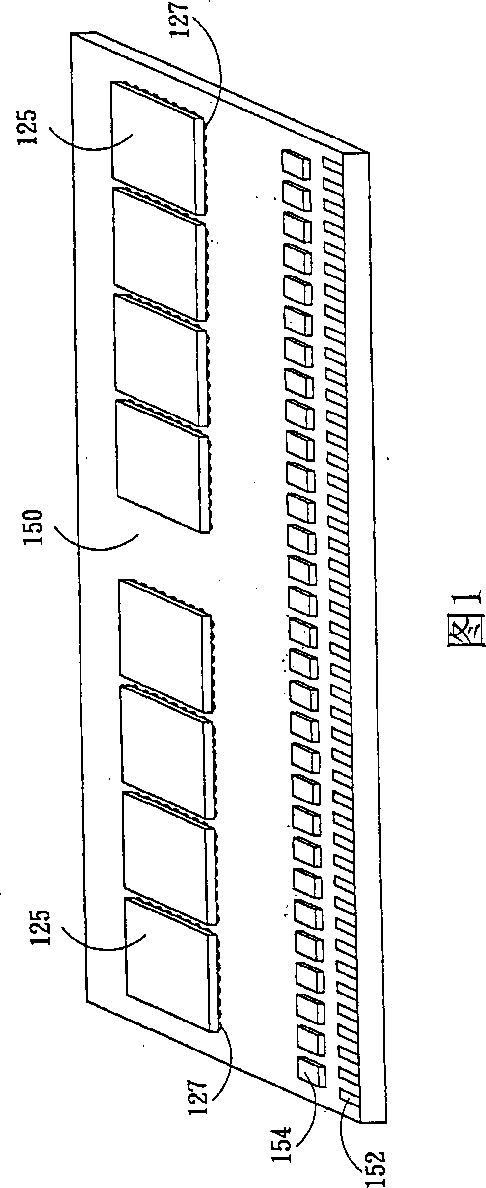
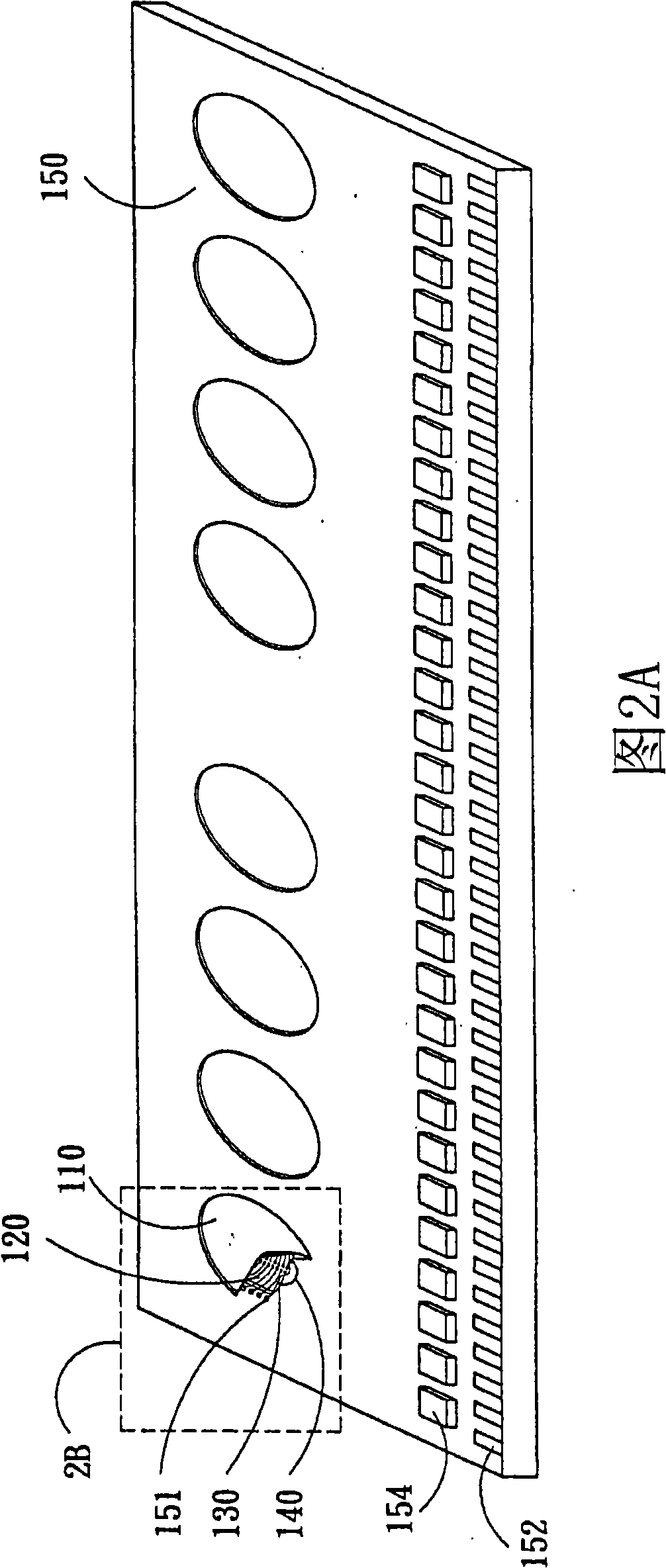
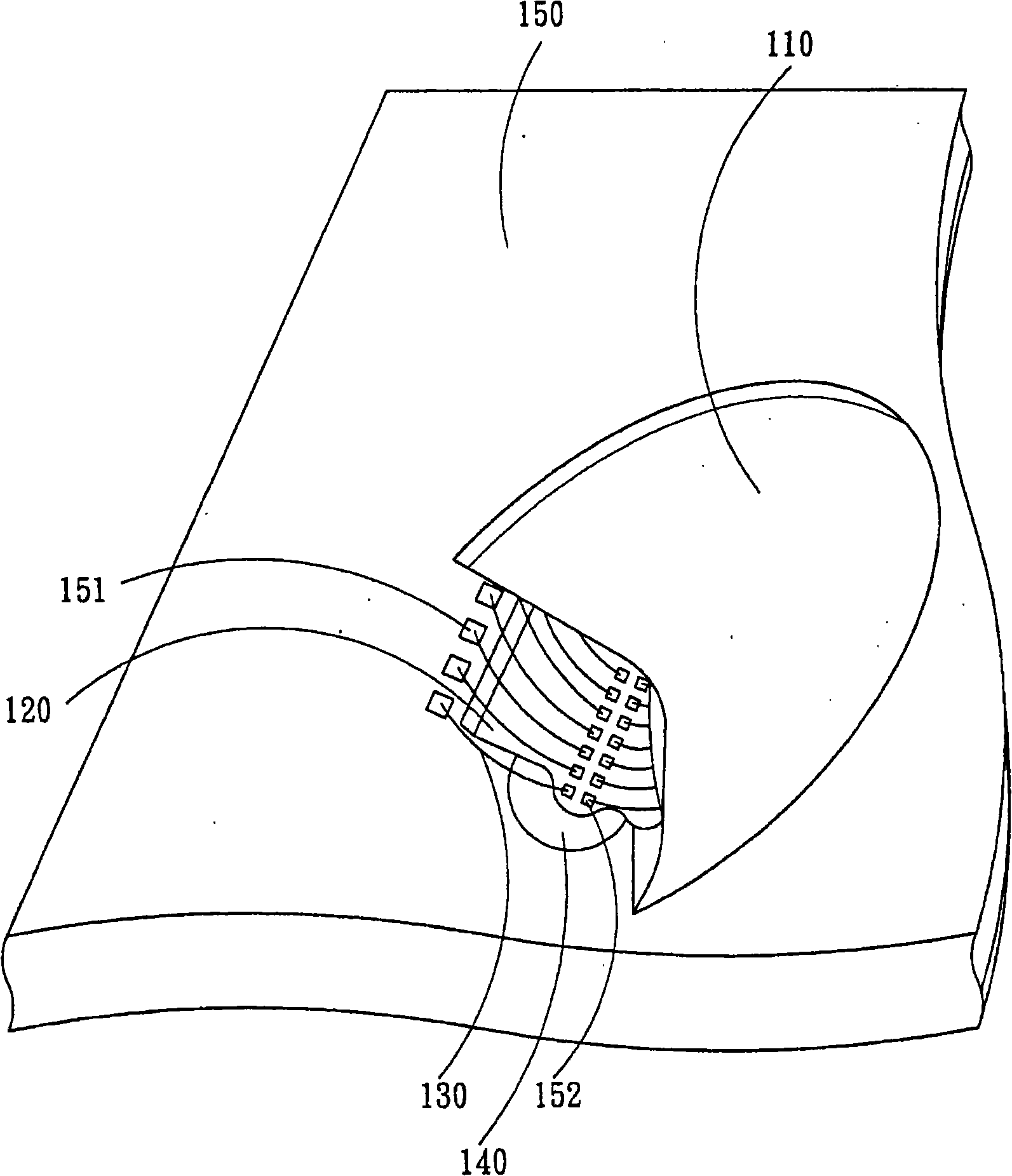
[0054] Some embodiments of the invention are described in detail below. However, the invention can be broadly practiced in other embodiments than this detailed description. That is, the scope of the present invention is not limited by the presented embodiments, but by the scope of the appended claims of the present invention. Secondly, when each element or structure in the diagrams of the embodiments of the present invention is described as a single element or structure, it should not be regarded as a limited cognition, that is, when the following description does not particularly emphasize the number limitation The spirit and scope of application can be extended to structures and methods in which multiple elements or structures coexist. Furthermore, in this specification, different parts of each element are not drawn in full scale, and some dimensions are exaggerated or simplified compared with other relevant dimensions, in order to provide a clearer description and enhance ...


PUM


Abstract

The invention relates to a memory module enclosure and an encapsulation method. A die, surrounding a chip, is arranged on a carrier plate to limit the flow and distribution range of fluid sealant and to equalize the thicknesses of the areas covered by the fluid sealant so as to avoid that pull to the enclosure is uneven after the fluid sealant in all the areas is solidified, thus preventing the enclosure from deforming due to uneven pull and improving the reliability of the enclosure. The invention uses the die to protect the leads during the fabrication process of the enclosure, thus preventing the leads from damages caused by collision.

Description

technical field [0001] The present invention relates to a packaging structure of a memory module and a packaging method thereof, in particular to a packaging structure of a memory module and a packaging method thereof produced by Chip On Board (COB for short). Background technique [0002] With the increasing popularity and multi-functionality of electronic products, memory modules are used in many electronic products, such as computers, mobile phones, PDAs, etc., resulting in an increasing demand for memory modules. As the demand increases, memory modules are also required Modules can have larger capacity and higher performance. Therefore, how to manufacture or package memory modules with large capacity, high performance and low cost has always been a major issue in the production and packaging of memory modules. [0003] Referring to FIG. 1 , it is a three-dimensional schematic diagram of a package structure of a general memory module on the market. Generally speaking, th...

Claims


Application Information

Patent Timeline
IPC IPC(8): H01L25/00H01L25/065H01L23/31H01L23/488H01L21/56H01L21/50H01L21/60H05K1/18H05K3/32G11C5/02G11C5/06
CPCH01L2224/45124H01L2224/73265H01L2224/48227H01L2224/32225H01L24/73
Inventor 苏忠志
Owner KUNSHAN HEISEI ELECTRONICS
Why Eureka
Try Eureka