Semiconductor device

A semiconductor and device technology, applied in the field of semiconductor devices, can solve the problems of high on-resistance saturation current, reduce the performance of high-power laterally diffused metal oxide semiconductor power transistors, etc., to reduce on-resistance and enhance the performance of high saturation current Effect

Inactive Publication Date: 2009-02-04
TAIWAN SEMICON MFG CO LTD
View PDF0 Cites 13 Cited by
  • Summary
  • Abstract
  • Description
  • Claims
  • Application Information

AI Technical Summary

Problems solved by technology

[0002] Semiconductor circuits like metal-oxide-semiconductor field-effect transistors (MOSFETs), suitable for high-power applications, suffer from high on-resistance
In MOSFET devices, such as high-power laterally diffused metal-oxide-semiconductor (LDMOS) structures, when a high voltage is applied to the gate, it produces high on-resistance and low saturation current in the channel under the gate, thereby reducing Performance of High Power Laterally Diffused Metal Oxide Semiconductor Power Transistors

Method used


Image

  • Semiconductor device
  • Semiconductor device
  • Semiconductor device

Examples


Embodiment Construction

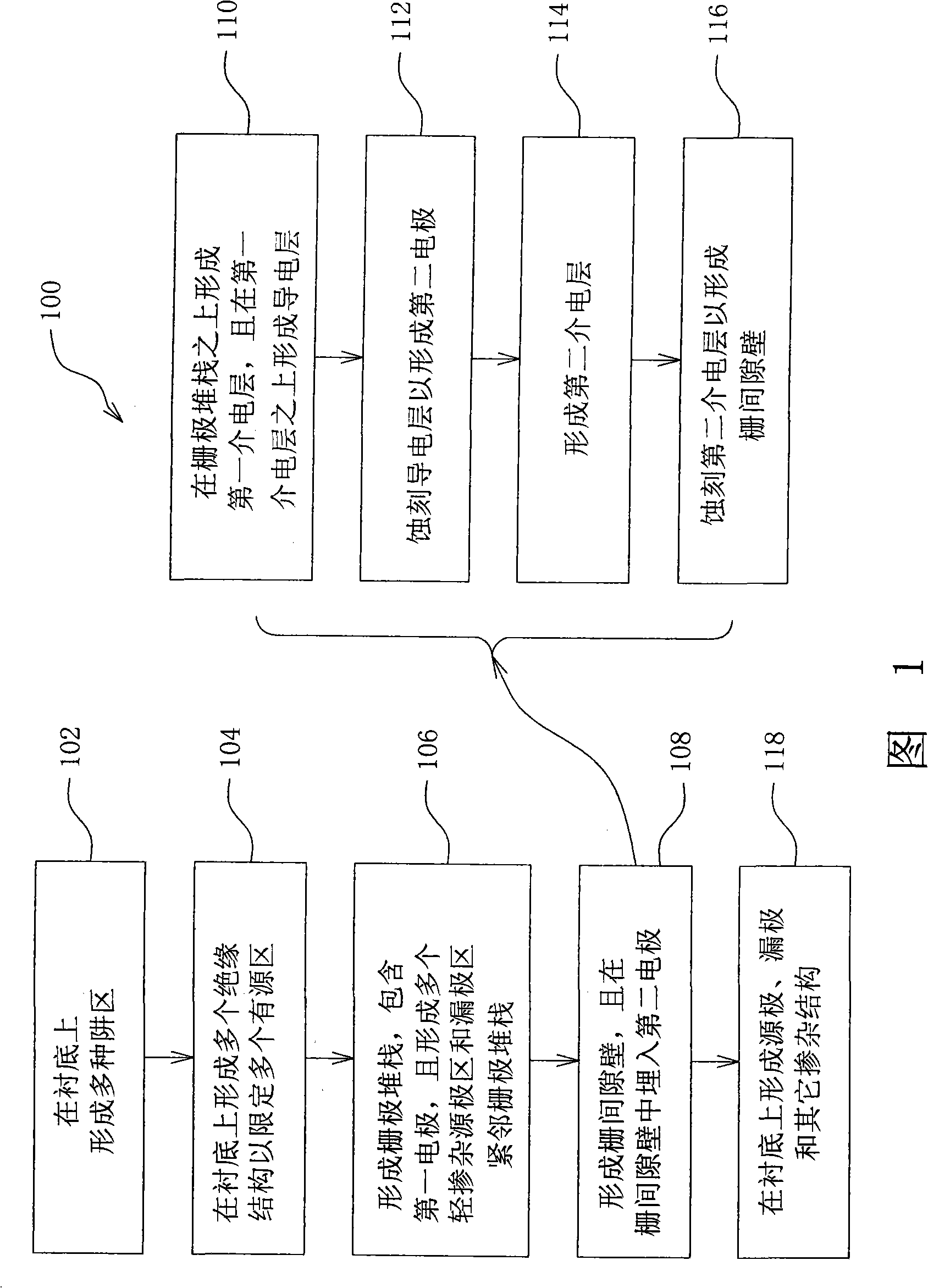
[0039] The invention relates to the field of semiconductor integrated circuits. In the description, many different embodiments or examples will be proposed to realize many different features of the present invention, and examples of specific components and arrangements are used to simplify the description of the content disclosed in the present invention. Of course, these embodiments and examples are for illustration only, and are not intended to limit the scope of the present invention. In addition, the purpose of reusing the same numbers or English letters in various examples and embodiments disclosed in the present invention is to simplify and clearly indicate the relationship between different embodiments and / or structures, but not to used to define its relationship. Moreover, in the following content, it is mentioned that a first feature is formed on a second feature, and its embodiments may include: an embodiment in which the first feature and the second feature are for...


PUM


Abstract

A semiconductor device includes a source region and a drain region disposed in a substrate wherein the source and drain regions have a first type of dopant; a gate electrode formed on the substrate interposed laterally between the source and drain regions; a gate spacer disposed on the substrate and laterally between the source region and the gate electrode, adjacent a side of the gate electrode; and a conductive feature embedded in the gate spacer.

Description

technical field [0001] The invention relates to the structure of a semiconductor integrated circuit, and in particular to a semiconductor device, which has a gate spacer structure of a buried conductive structure. Background technique [0002] Semiconductor circuits, such as Metal Oxide Semiconductor Field Effect Transistors (MOSFETs), are suitable for high power applications, but suffer from high on-resistance. In MOSFET devices, such as high-power laterally diffused metal-oxide-semiconductor (LDMOS) structures, when a high voltage is applied to the gate, it produces high on-resistance and low saturation current in the channel under the gate, thereby reducing performance of high power laterally diffused metal oxide semiconductor power transistors. Contents of the invention [0003] The technical problem to be solved by the present invention is to provide a semiconductor device that can increase the saturation current and reduce the on-resistance. [0004] In order to ac...

Claims


Application Information

Patent Timeline
Patent Type & Authority Applications(China)
IPC IPC(8): H01L29/78H01L29/423
CPCH01L29/66689H01L29/0878H01L21/26586H01L29/086H01L29/7816H01L29/402H01L29/7817
Inventor 陈郁文陈富信黄宗义蔡泳田
Owner TAIWAN SEMICON MFG CO LTD
Why Eureka
Try Eureka