Method for testing FPGA device

A device and testing machine technology, applied in the direction of digital circuit testing, electronic circuit testing, instruments, etc., to achieve the effect of realizing industrialized testing, reducing operation links and improving testing efficiency

Inactive Publication Date: 2009-02-11
BEIJING CHIPADVANCED
View PDF0 Cites 30 Cited by
  • Summary
  • Abstract
  • Description
  • Claims
  • Application Information

AI Technical Summary

Problems solved by technology

However, how to make full use of the resources of the integrated circuit testing machine to realize the fast and effective configuration of FPGA devices, and then carry out industrial testing still has many technical problems that need to be solved

Method used


Image

  • Method for testing FPGA device
  • Method for testing FPGA device
  • Method for testing FPGA device

Examples


Embodiment Construction

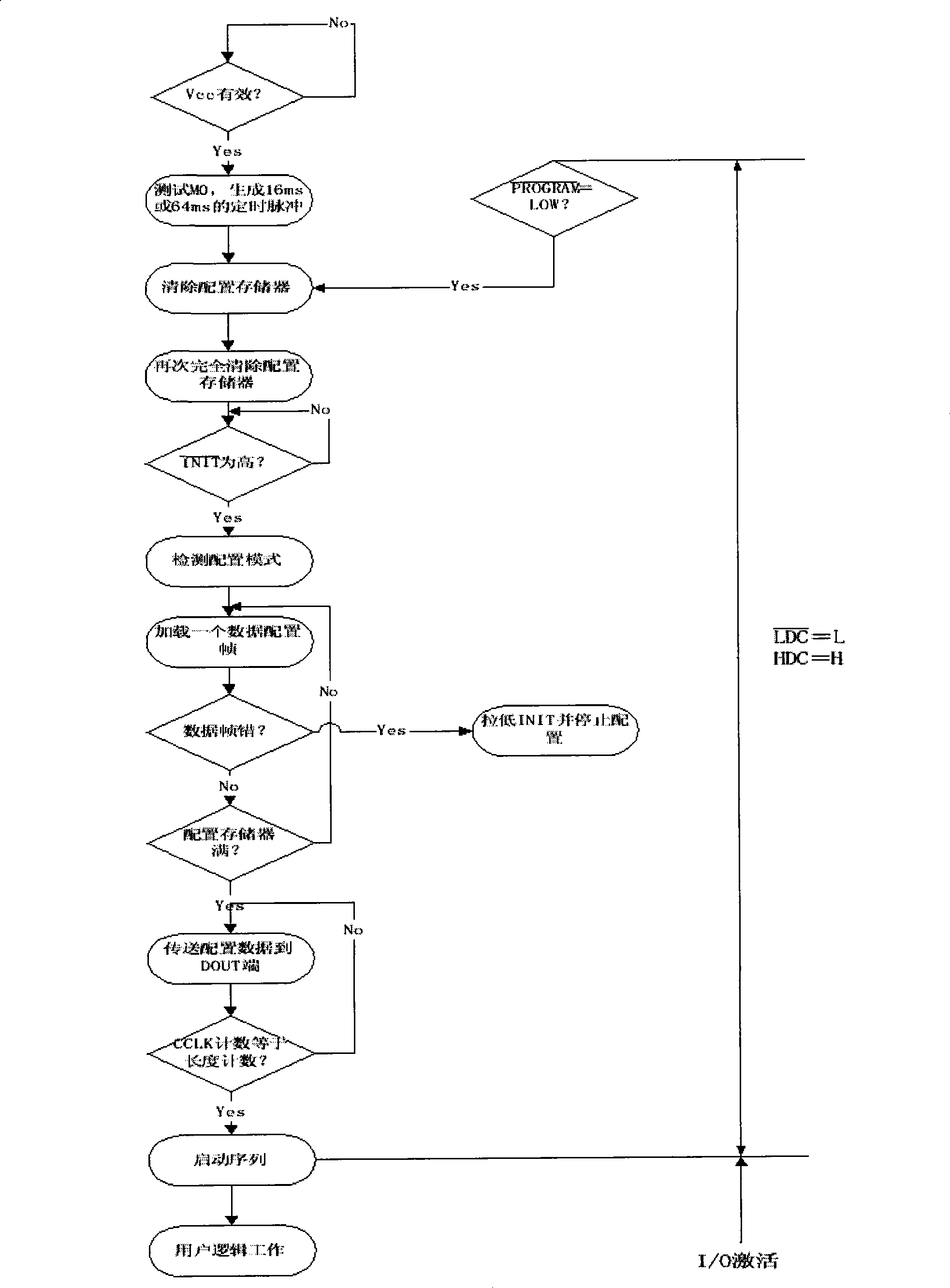
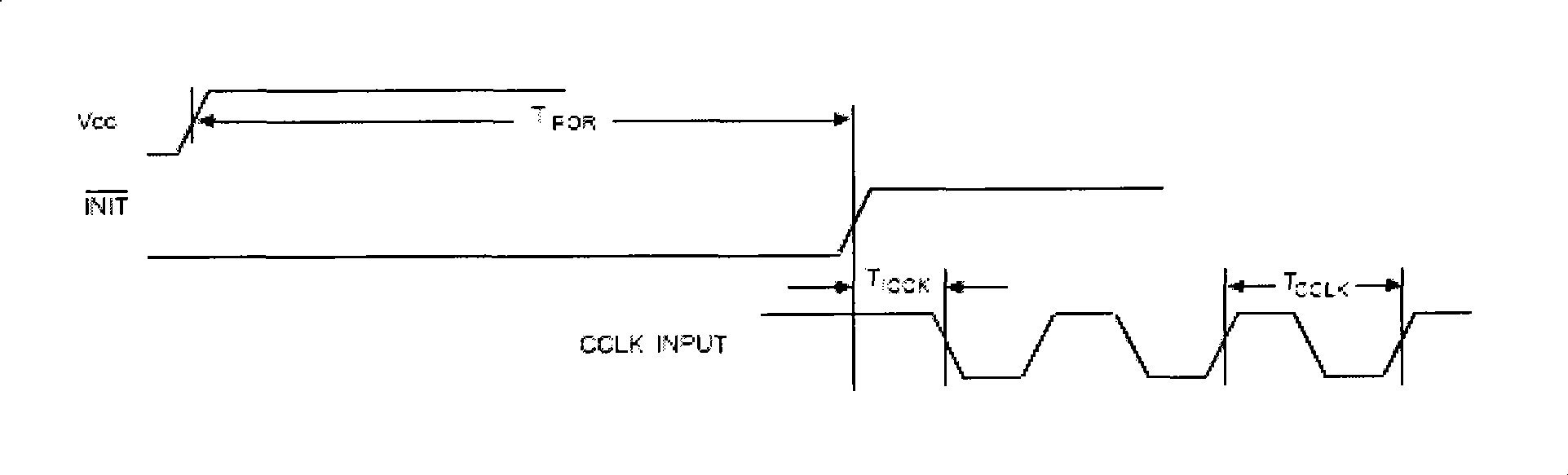
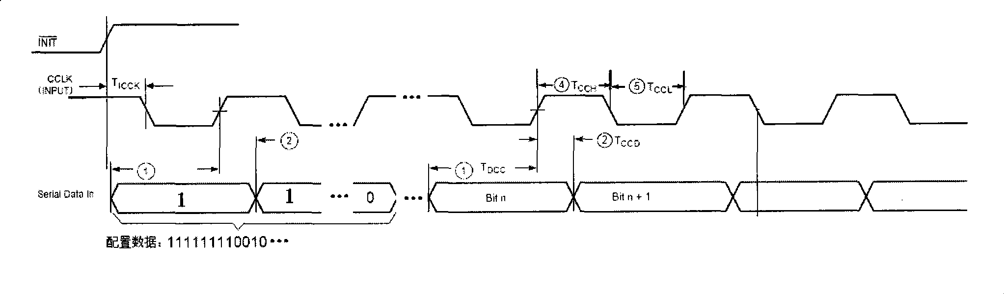
[0029] The problem to be solved by the invention is how to use the existing integrated circuit testing machine to perform the industrialized testing task of the FPGA device. At present, the number of pins of more advanced FPGA devices exceeds 1000, requiring the integrated circuit tester to have more channels than the number of pins of the FPGA device under test, or to have the function of channel multiplexing. For FPGA devices, the length of the test vector for each test is determined by the complexity of the configuration circuit and the purpose of the test, and the length of the test vectors for each test is different. For example, the length of the test vector of the configuration file of the Xilinx4010E FPGA device series device is 178k lines, and the length of the test vector varies during the test process. To test FPGA devices, it is necessary to repeat many "configuration-test" processes. Therefore, the test vector space depth of the integrated circuit tester is requir...


PUM


Abstract

The invention discloses a method for testing a FPGA device, which comprises the following steps of (1) generating a configuration file for configuring predetermined function to the FPGA device; (2) subjecting the FPGA device to a configuration step; (3) extracting configuration information from the configuration file and carrying out data conversion to obtain a configuration data signal of a predetermined pin; (4) arranging the logic state of each control pin in the FPGA device, and arranging the time sequence information of each pin to obtain the testing vector of the configuration process; (5) arranging the signal variation time of each pin based on the time sequence information of each pin to obtain a test pattern; and (6) carrying out the test pattern for completing the test working. With the invention, the prior integrated circuit tester can be employed for testing the FPGA device, so as to not only reduce the operation steps, but also improve the test efficiency and facilitate for the industrialization testing of the FPGA device.

Description

technical field [0001] The invention relates to a method for implementing industrialized testing by using an integrated circuit testing machine to configure FPGA devices (Field Programmable Gate Array, Field Programmable Gate Array), and belongs to the technical field of integrated circuit testing. Background technique [0002] The FPGA device is a new type of programmable logic device that appeared in the mid-1980s. It appeared as a semi-custom circuit in the field of application-specific integrated circuits (ASIC). The disadvantage of the limited number of programming device gates can be widely used in aerospace, communications, computer hardware systems, program control, digital system test and diagnosis and other fields. The FPGA device adopts the new concept of logic cell array LCA (Logic Cell Array), which includes three parts: configurable logic module CLB (Configurable Logic Block), input and input module IOB (Input Output Block) and internal wiring (Interconnect). ...

Claims


Application Information

Patent Timeline
Patent Type & Authority Applications(China)
IPC IPC(8): G01R31/317G01R31/3177G01R31/3183
Inventor 吉国凡张琳刘炜赵智昊王慧石志刚孙博金兰李尔孙杨陈希
Owner BEIJING CHIPADVANCED
Why Eureka
Try Eureka