Plasma flat light source structure and LCD device

A technology for liquid crystal display devices and planar light sources, which is applied in gas plasma lamps, optics, nonlinear optics, etc., can solve the problems of high cost of filter material layers and rising manufacturing costs of plasma planar light source structures, and achieve improved color purity and excellent The effect of display quality

Inactive Publication Date: 2009-02-18
CPT TECH GRP
View PDF0 Cites 2 Cited by
  • Summary
  • Abstract
  • Description
  • Claims
  • Application Information

AI Technical Summary

Problems solved by technology

However, due to the high cost of making the filter material layer, the manufacturing cost of the plasma planar light source structure will increase.

Method used


Image

  • Plasma flat light source structure and LCD device
  • Plasma flat light source structure and LCD device
  • Plasma flat light source structure and LCD device

Examples


no. 1 example

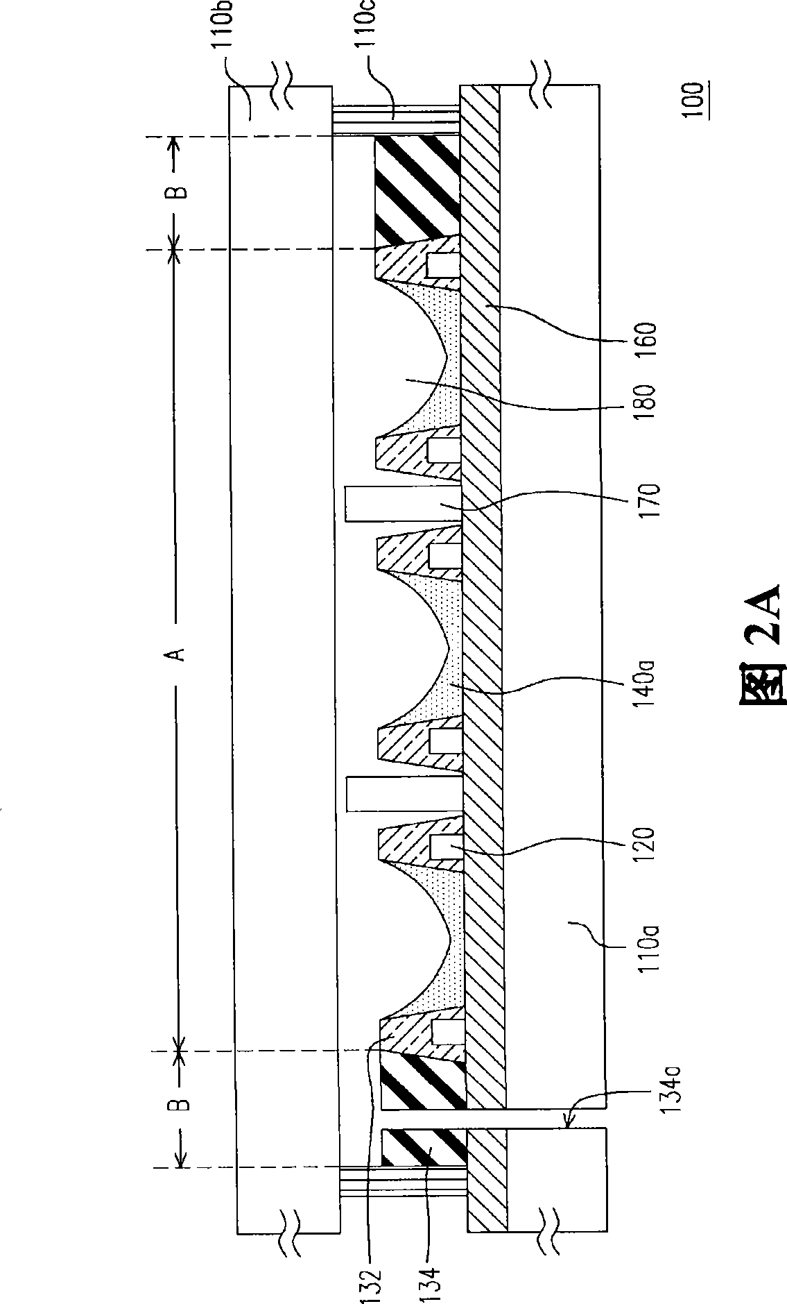
[0069] Fig. 2A is a schematic structural diagram of the plasma planar light source structure of the first embodiment. 2A, the plasma planar light source structure 100 includes a first substrate 110a, a plurality of electrode lines 120, a plurality of dielectric patterns 132, a dielectric layer 134, a first fluorescent material layer 140a, a second substrate 110b and a sealant 110c. The installation positions and materials of each component will be described below.

[0070] The first substrate 110a has a light emitting area A and a peripheral area B surrounding the light emitting area A. As shown in FIG. The electrode lines 120 are disposed on the first substrate 110a and extend from the peripheral area B to the light emitting area A. As shown in FIG. The dielectric patterns 132 are disposed on the first substrate 110a, and each dielectric pattern 132 covers the electrode lines 120 therein. The dielectric layer 134 covers the peripheral area B of the first substrate 110a, whe...

no. 2 example

[0080] Fig. 3A is a schematic structural view of the plasma planar light source structure of the second embodiment, Figure 3B It is a top view of the partition wall of the plasma planar light source structure in FIG. 3A . Please refer to FIG. 3A , the plasma planar light source structure 200 is similar to the above-mentioned plasma planar light source structure 100 , the difference is that: the plasma planar light source structure 200 also includes a second fluorescent material layer 140 b and a partition wall 210 . The second fluorescent material layer 140b is disposed on the second substrate 110b, and includes red, green and blue fluorescent materials, for example. When ultraviolet rays irradiate the second fluorescent material layer 140b, the red, green and blue fluorescent materials in the second fluorescent material layer 140b will also emit red, green and blue light, so as to mix colors to form white light. The partition wall 210 is disposed on the second substrate 110b...

no. 3 example

[0084] Fig. 4A is a schematic structural diagram of the plasma planar light source structure of the third embodiment, Figure 4B It is a top view of the first partition wall of the plasma planar light source structure in FIG. 4A . Please refer to Figure 4A together with Figure 4B , the plasma planar light source structure 300 is similar to the plasma planar light source structure 100 of the first embodiment, the difference is that: the plasma planar light source structure 300 does not have the dielectric layer 134 , but has the first partition wall 312 . The first partition wall 312 is disposed on the peripheral region B of the first substrate 110a, and the first substrate 110a inside the first partition wall 312 has a through hole 320 therein. The first partition wall 312 is fabricated on the first substrate 110a by, for example, screen printing technology or other suitable methods. In addition, the first partition wall 312 has a first notch 312a, and the first notch 312a ...


PUM


Abstract

Provided are a plasma plane light source structure and a LCD device, the plasma plane light source structure comprises a first base plate having a luminous zone and a peripheral zone enclosing around the luminous zone; a plurality of electrode wires arranged on the first base plate and extending to the luminous zone from the peripheral zone; a plurality of dielectric patterns arranged on the first base plate, in which, any one dielectric pattern can be covered on the any other one; a first division wall arranged in the peripheral zone, in which, a through hole is provided in the first base plate in the internal of the first division wall; a first fluorescent material layer arranged on the surfaces of the dielectric patterns, in which, the first fluorescent material layer is also arranged in the peripheral zone of the first base plate, but the first fluorescent material layer is not arranged on the first base plate in the internal of the first division wall; a second base plate arranged above the first base plate; and seal objects arranged between the first base plate and the second base plate and positioned on the edges of the first base plate and the second base plate.

Description

[0001] This application is a divisional application of the invention patent application with the application number "200610007810.5" and the invention title "plasma planar light source structure and liquid crystal display device" submitted by the applicant on February 17, 2006. technical field [0002] The present invention relates to a flat light source structure, and in particular to a plasma flat light source structure applicable to liquid crystal displays. Background technique [0003] With the development of the industry, digital tools such as mobile phones, digital cameras, notebook computers, and desktop computers are all developing in the direction of more convenience, more functions and more beautiful appearance. The display screens of these electronic products are indispensable human-machine communication interfaces, and the display screens of the above-mentioned products can bring more operation convenience to users. In recent years, most of the display screens on...

Claims


Application Information

Patent Timeline
Patent Type & Authority Applications(China)
IPC IPC(8): H01J63/08G02F1/13357G02F1/1333G02F1/1335
Inventor 张昭仁吕德助
Owner CPT TECH GRP
Why Eureka
Try Eureka