Multi-light beam coupling high power semiconductor laser unit

A laser device and semiconductor technology, applied in the direction of semiconductor laser devices, laser devices, etc., can solve the problems of complex adjustment, reduced efficiency, large divergence angle, etc.

Inactive Publication Date: 2009-02-18
CHANGCHUN INST OF OPTICS FINE MECHANICS & PHYSICS CHINESE ACAD OF SCI
View PDF0 Cites 6 Cited by
  • Summary
  • Abstract
  • Description
  • Claims
  • Application Information

AI Technical Summary

Problems solved by technology

This structure can achieve beam combining, but the disadvantages are: (1) The two lasers are placed vertically at 90°, and the adjustment is complicated; (2) The cube polarization coupling prism is used, and the middle glued surface melts the glue during long-term high-power use, which improves the efficiency. (3) Due to the large divergence angle of the semiconductor laser itself without collimation, the efficiency of directly placing the half-wave plate to rotate the polarization direction is reduced

Method used


Image

  • Multi-light beam coupling high power semiconductor laser unit
  • Multi-light beam coupling high power semiconductor laser unit
  • Multi-light beam coupling high power semiconductor laser unit

Examples


Embodiment Construction

[0013] The present invention will be described in further detail below in conjunction with the embodiment given with accompanying drawing.

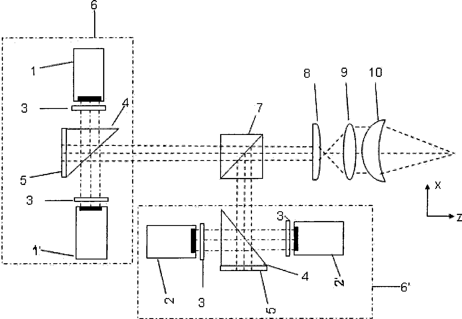
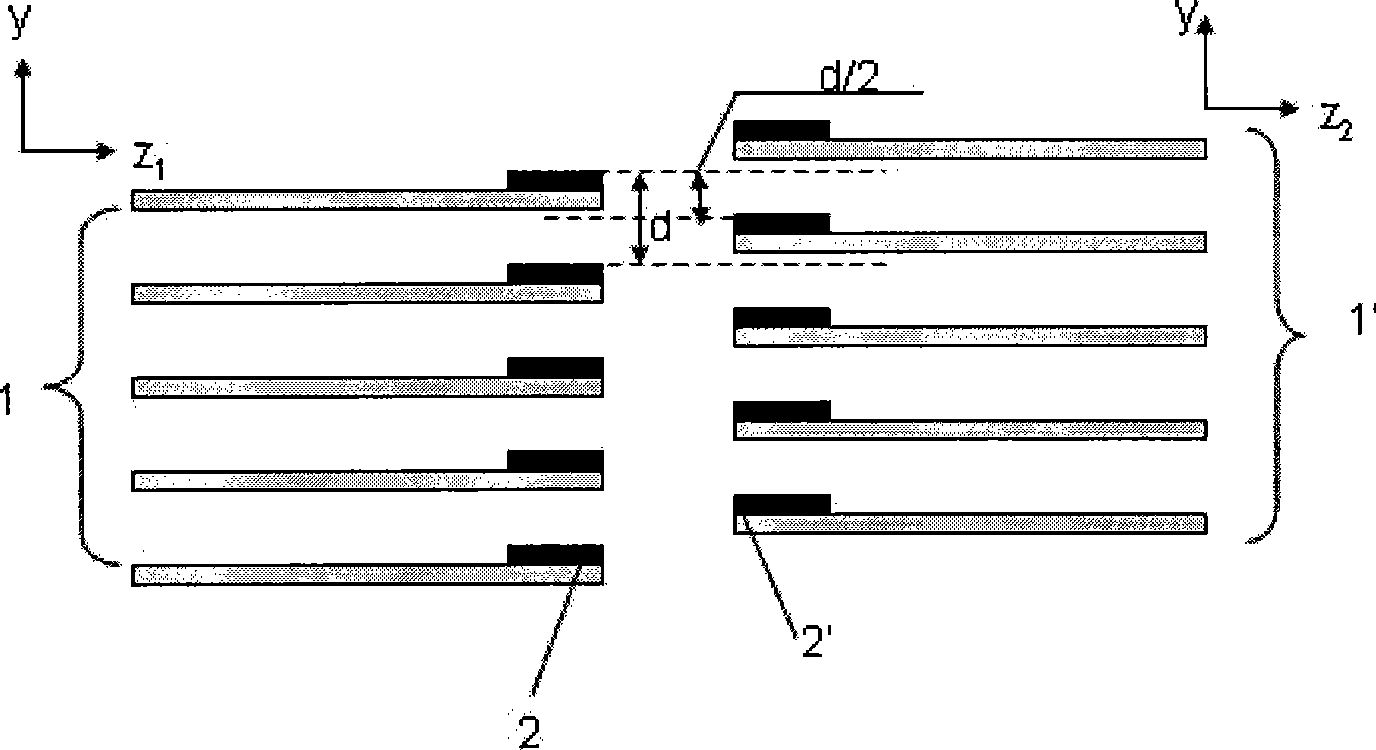
[0014] refer to figure 1 , a multiple beam coupling high-power semiconductor laser device, including four semiconductor lasers 1, 1', 2, 2' of the same polarization state, a wavelength selection element 7, and a beam expander focusing device, the four semiconductor lasers of the same polarization state The wavelength of the two semiconductor lasers 1, 1' in the laser is λ 1 , the wavelength of the other two semiconductor lasers 2, 2' is λ 2 ; Take the wavelength of the four semiconductor lasers as λ 1 The two semiconductor lasers 1, 1' form a group, and the wavelength is λ 2 The two semiconductor lasers are another group, which respectively form two beam coupling light sources 6, 6' through polarization coupling devices; the two beam coupling light sources 6, 6' are placed perpendicular to each other, and the The wavelength selection...


PUM


Abstract

The invention relates to high-power semiconductor laser device preparation technology, especially a multiple light beam coupling high-power semiconductor laser device, including four semiconductor laser devices with identical polarization state, a wavelength selection element, a beam-expanding focusing device. The wavelength of two semiconductor laser devices of the four semiconductor laser devices is Lambada1, and the wavelength of another two is Lambada2; the two semiconductor laser devices with same wavelength as a group, and the another two semiconductor laser devices with same wavelength as the other group, wherein the two groups form two light beam coupling light sources by a polarization coupled device; the two light beam coupling light sources are coupled into a beam by the wavelength selection element, to transmit to the beam-expanding focusing device to send out. The invention provides most advanced and feasible preparation technology for correlation technique field of demand on ultra-high-power semiconductor laser device until today.

Description

technical field [0001] The invention relates to a high-power semiconductor laser preparation technology, in particular to a high-power semiconductor laser device realized by coupling beams of multiple semiconductor laser light sources. Background technique [0002] Compared with other types of lasers, semiconductor lasers (LD) have the advantages of small size, light weight, high efficiency, long life, and direct current modulation, so they are widely used in many fields such as industry, military, nuclear energy, and communications. The requirements for output power and brightness of semiconductor lasers are also getting higher and higher. By integrating the semiconductor laser light-emitting unit into a one-dimensional line array (LD Bar) and a two-dimensional array (LD Stack) stacking multiple LD Bars, the output power of the semiconductor laser can be effectively improved, but due to the limitation of heat dissipation, the two Dimensional area arrays cannot stack LD Bar...

Claims


Application Information

Patent Timeline
Patent Type & Authority Applications(China)
IPC IPC(8): H01S5/40
Inventor 顾媛媛彭航宇单肖楠王立军刘云王祥鹏
Owner CHANGCHUN INST OF OPTICS FINE MECHANICS & PHYSICS CHINESE ACAD OF SCI
Why Eureka
Try Eureka