Manufacturing method of opto-electric hybrid board and opto-electric hybrid board obtained thereby

a technology of opto-electric hybrid boards and manufacturing methods, which is applied in the field of manufacturing methods of opto-electric hybrid boards and opto-electric hybrid boards obtained thereby, can solve the problems of affecting the quality of optical coupling, the sensitivity of optical waveguides and boards, and the difficulty of providing good accuracy, so as to achieve high accuracy, facilitate high accuracy, and provide optical coupling high accuracy

Inactive Publication Date: 2009-08-20
NITTO DENKO CORP
View PDF3 Cites 18 Cited by
  • Summary
  • Abstract
  • Description
  • Claims
  • Application Information

AI Technical Summary

Benefits of technology

[0015]The present inventor has diligently made studies of a method of optically coupling light-emitting and light-receiving elements mounted on an electrical wiring board and an optical waveguide provided in an optical wiring board to each other easily with high accuracy. As a result, the present inventor has found that the light-emitting and light-receiving elements and the optical waveguide are optically coupled to each other easily with high accuracy by using a metal substrate for each of the electrical wiring board and the optical wiring board and by the process of forming alignment openings in the electrical wiring board and the optical wiring board by lithography, and then fitting and fixing guide pins in the alignment openings. Thus, the present inventor has attained the present invention.
[0016]In the method of manufacturing the opto-electric hybrid board according to the first aspect of the present invention, the alignment openings are formed by photolithography in the electrical wiring board and the optical wiring board as described above, and are fixed coaxially with the single guide pin. This accomplishes the positioning of the electrical wiring board and the optical wiring board easily and accurately to provide optical coupling with high accuracy. Additionally, the above-mentioned electrical wiring board has the advantage of correctly positioning the above-mentioned alignment openings and a conductor pattern of pads, interconnect lines and the like because the alignment openings and the conductor pattern are formed at the same time by using a single photomask. Similarly, the above-mentioned optical wiring board has the advantage of correctly positioning the above-mentioned alignment openings and optical coupling openings because the alignment openings and the optical coupling openings are formed at the same time by using a single photomask. The use of the metal substrate for the electrical wiring board and the optical wiring board offers the advantage of providing high dimensional stability of the boards to allow the stable retention of the arrangement of the above-mentioned correctly positioned members. This eliminates the need for conventional cumbersome and complicated labor to achieve high-accuracy optical coupling, thereby significantly reducing manufacturing costs and operating time.
[0017]In the method of manufacturing the opto-electric hybrid board according to the second aspect of the present invention, the strip-shaped metal substrate has the first end provided with the electrical wiring board portion and the second end provided with the optical wiring board portion. The alignment openings are formed in the board portions in a manner similar to that described above, and the strip-shaped metal substrate is folded back. The electrical wiring board portion and the optical wiring board portion in a stacked relation are fixed coaxially with the guide pins. This accomplishes the positioning of the electrical wiring board portion and the optical wiring board portion easily and accurately to provide optical coupling with high accuracy. Additionally, this method has the advantage of correctly positioning the alignment openings and optical coupling openings because the alignment openings in the above-mentioned electrical wiring board portion and the optical wiring board portion and the optical coupling openings in the optical wiring board portion are formed at the same time by using a single photomask. Since the electrical wiring board portion and the optical wiring board portion are constructed by the common metal substrate, the method offers the advantage of providing high dimensional stability of the boards to allow the stable retention of the arrangement of the above-mentioned correctly positioned members. This eliminates the need for conventional cumbersome and complicated labor to achieve high-accuracy optical coupling, thereby significantly reducing manufacturing costs and operating time.
[0018]The opto-electric hybrid boards obtained by these manufacturing methods are capable of transmitting light with high efficiency because the optical coupling is achieved, with the electrical wiring board and the optical wiring board to be stacked being positioned with high accuracy.

Problems solved by technology

However, a series of positioning processes involving image processing as described above not only require very cumbersome and complicated labor but also present a problem such that the optical waveguide and the board are liable to be deformed by heat and tension during processing and during lamination and bonding, thereby finding difficulties in providing good accuracy.

Method used


Image

  • Manufacturing method of opto-electric hybrid board and opto-electric hybrid board obtained thereby
  • Manufacturing method of opto-electric hybrid board and opto-electric hybrid board obtained thereby
  • Manufacturing method of opto-electric hybrid board and opto-electric hybrid board obtained thereby

Examples


example 1

[0089]An opto-electric hybrid board was manufactured in a manner similar to the present invention described above (with reference to FIGS. 1 to 17), more specifically in a manner to be described below.

[0090](1) Production of Electrical Wiring Board

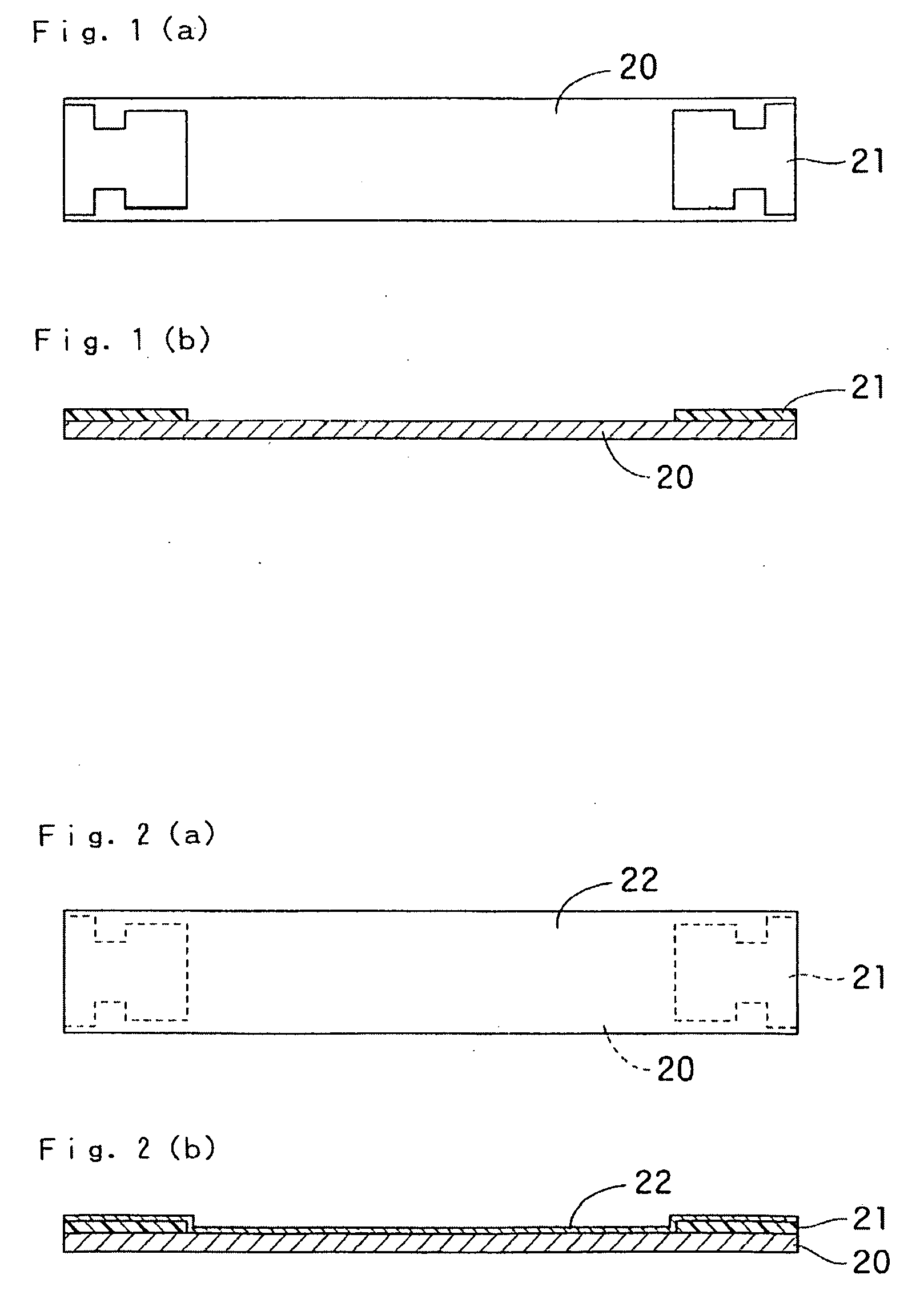
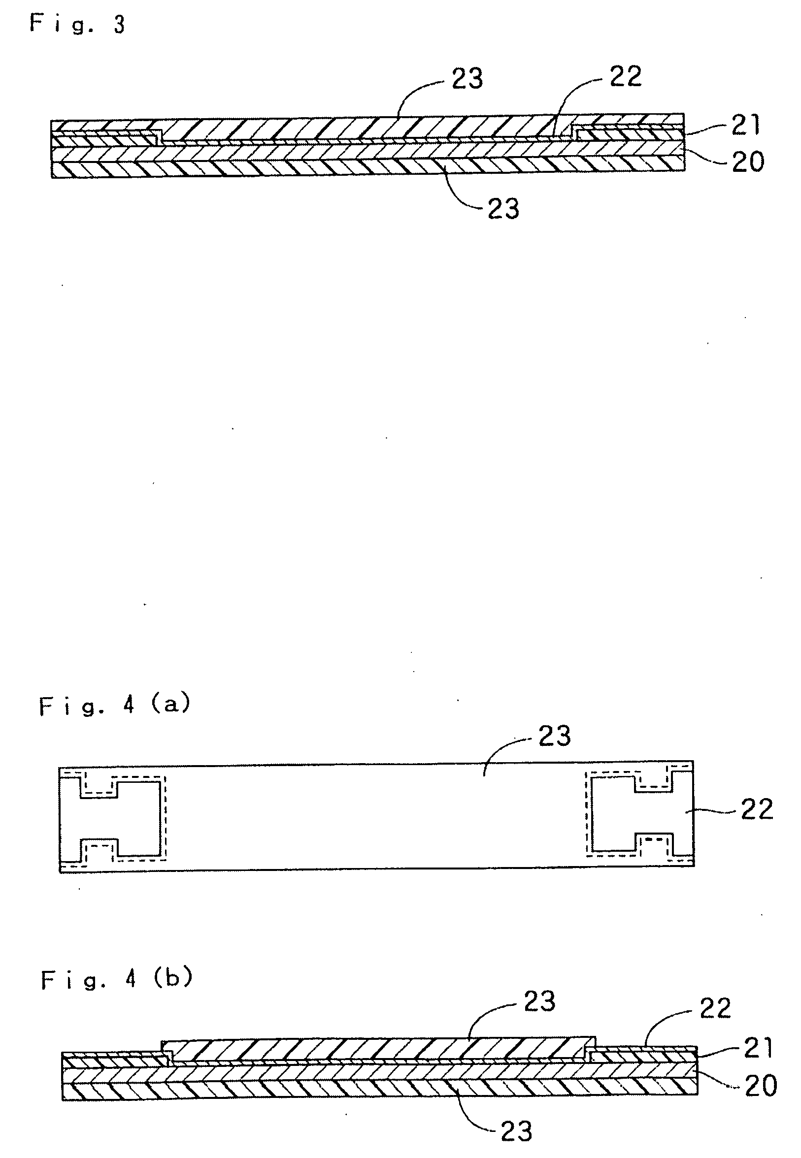
[0091]A photosensitive polyimide having a thickness of 10 μm was applied onto an SUS substrate having a thickness of 0.025 mm, a width of 50 mm and a length of 150 mm. Thereafter, a future insulation layer portion was exposed to light by using a photomask. Thus, a difference was made in solubility between an exposed portion and an unexposed portion of the polyimide by lower-layer PEB. Then, the unexposed portion was removed by using a developing solution. Thereafter, polyimide cure was performed by heating, and the cured exposed portion functioned as an insulation layer as shown in FIGS. 1(a) and 1(b).

[0092]Next, a sputtering apparatus was used to form a Cu / NiCr seed layer (having a Cu thickness of 0.15 μm and a NiCr thickness of 0.15 μm) ...

example 2

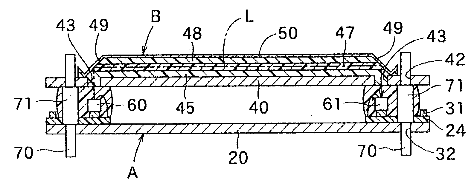
[0112]A strip-shaped SUS substrate having a thickness of 0.025 mm, a width of 50 mm and a length of 300 mm was prepared. One end portion of the strip-shaped SUS substrate was adapted for use as an electrical wiring board portion, and the other end portion thereof was adapted for use as an optical wiring board portion. Alignment openings in a portion for use as the electrical wiring board portion and in a portion for use as the optical wiring board portion, and optical coupling openings in the portion for use as the optical wiring board portion were produced at the same time by photolithography and SUS etching as shown in FIG. 19(a). Except for this, Example 2 was similar to Example 1 described above to produce the components of the electrical wiring board portion and the components of the optical wiring board portion. The electrical wiring board portion and optical wiring board portion described above were produced so that the surfaces of the respective portions were on opposite sid...


PUM

PropertyMeasurementUnit
thicknessaaaaaaaaaa
thicknessaaaaaaaaaa
thicknessaaaaaaaaaa

Abstract

A method of manufacturing an opto-electric hybrid board capable of optically coupling light-emitting and light-receiving elements mounted on an electrical wiring board and an optical waveguide provided in an optical wiring board to each other easily with high accuracy. An opto-electric hybrid board obtained thereby. Guide pins have end portions fitted in alignment openings of an electrical wiring board and end portions fitted in alignment openings of an optical wiring board to accomplish alignment therebetween. The electrical wiring board is configured such that a conductor layer having pads for mounting light-emitting and light-receiving elements thereon and interconnect lines is formed on a metal substrate, and the alignment openings are formed in the metal substrate. The optical wiring board is configured such that an optical waveguide is formed on a metal substrate, and optical coupling openings for the optical waveguide and the alignment openings are formed in the metal substrate.

Description

RELATED APPLICATIONS[0001]This application claims the benefit of U.S. Provisional Application No. 61 / 042,082, filed Apr. 3, 2008, which is hereby incorporated by reference.BACKGRROUND OF THE INVENTION[0002]1. Field of the Invention[0003]The present invention relates to a method of manufacturing an opto-electric hybrid board which has found wide use in a variety of electric and electronic technologies using optics such as optical communications, optical information processing and the like, and to an opto-electric hybrid board obtained thereby.[0004]2. Description of the Related Art[0005]In recent years, rapid advances in technologies regarding optical communications, optical information processing and the like have led to increasing demand for an opto-electric hybrid board in which optical interconnect lines (an optical waveguide) and electrical interconnect lines (a metallization pattern) are combined on the same board.[0006]An example of the above-mentioned opto-electric hybrid boa...

Claims


Application Information

Patent Timeline
Patent Type & Authority Applications(United States)
IPC IPC(8): G02B6/13G02B6/42G03F7/20
CPCG02B6/10G02B6/1221G02B6/136G02B6/42G02B6/4214H01L2224/16225G02B6/43H05K1/0274H05K1/056H05K1/144G02B6/4231G02B6/13
Inventor HODONO, MASAYUKI
Owner NITTO DENKO CORP
Why Eureka
Try Eureka