Integrated surface mode biosensor

a biosensor and integrated technology, applied in the field of biological, biochemical or chemical sensing and/or particle detection, can solve the problems of very lossy waveguide mode, and achieve the effects of high tuneability, high integration, and high optical sensitiveness

Inactive Publication Date: 2009-04-23
INTERUNIVERSITAIR MICRO ELECTRONICS CENT (IMEC VZW) +1
View PDF18 Cites 17 Cited by
  • Summary
  • Abstract
  • Description
  • Claims
  • Application Information

AI Technical Summary

Benefits of technology

[0003]It is an object of aspects of the present invention to provide alternative or good surface mode based, such as e.g. surface plasmon based, detection systems and methods. An advantage of embodiments of this invention is the provision of surface mode based detection systems, e.g. plasmon based detection systems, such as biosensors, biochemical sensors and chemical sensors that are small, e.g. fit in a lab-on-chip application. It is furthermore an advantage of embodiments of the present invention to provide surface mode based detection systems, e.g. plasmon based detection systems and methods that are highly tuneable. An advantage of embodiments of the present invention is the tuning of surface mode based detection systems and methods, e.g. surface plasmon based detection systems and methods, for example tuning them to desired wavelength ranges and/or to a desired range of analyte refractive indices. It is furthermor...

Problems solved by technology

However, all integrated SPR sensors that have been investigated so far typically have dimensions of wave guides and optical components tha...

Method used


Image

  • Integrated surface mode biosensor
  • Integrated surface mode biosensor
  • Integrated surface mode biosensor

Examples


example 1

[0082]In a first example, a comparison is shown between an experimental result and simulation result for a system wherein a 5 μm strip of a gold layer is used. The strip is provided by etching in a silicon substrate with a depth of 80.62 nm and by providing a gold layer with a thickness of 49.74 nm. Measurements are performed in plain air. In FIG. 9a and 9b a comparison of the measured and calculated transmission as function of wavelength is shown. A good qualitative agreement can be seen between the measured and simulated results. The discrepancy between the results may be due to the fact that the etch process is not optimised for the silicon substrate used and the fact that small variations in the thickness and roughness of the gold layer may be present. The relative large measured losses are due to the roughness of the etching and the consequent roughness of the deposited gold layer.

[0083]A plurality of examples is provided illustrating simulated results obtainable with a Mach-Ze...

example 2

[0084]Example 2 illustrates simulated results obtainable with a Mach-Zehnder Surface Plasmon interferometer using a sensor having a silicon-on-insulator (SOI) substrate with an embedded gold (Au) layer. The parameters of the different components of the input wave guide structure and sensing wave guide structure used in the simulation, as well as the length of the sensing section are indicated in table 1.

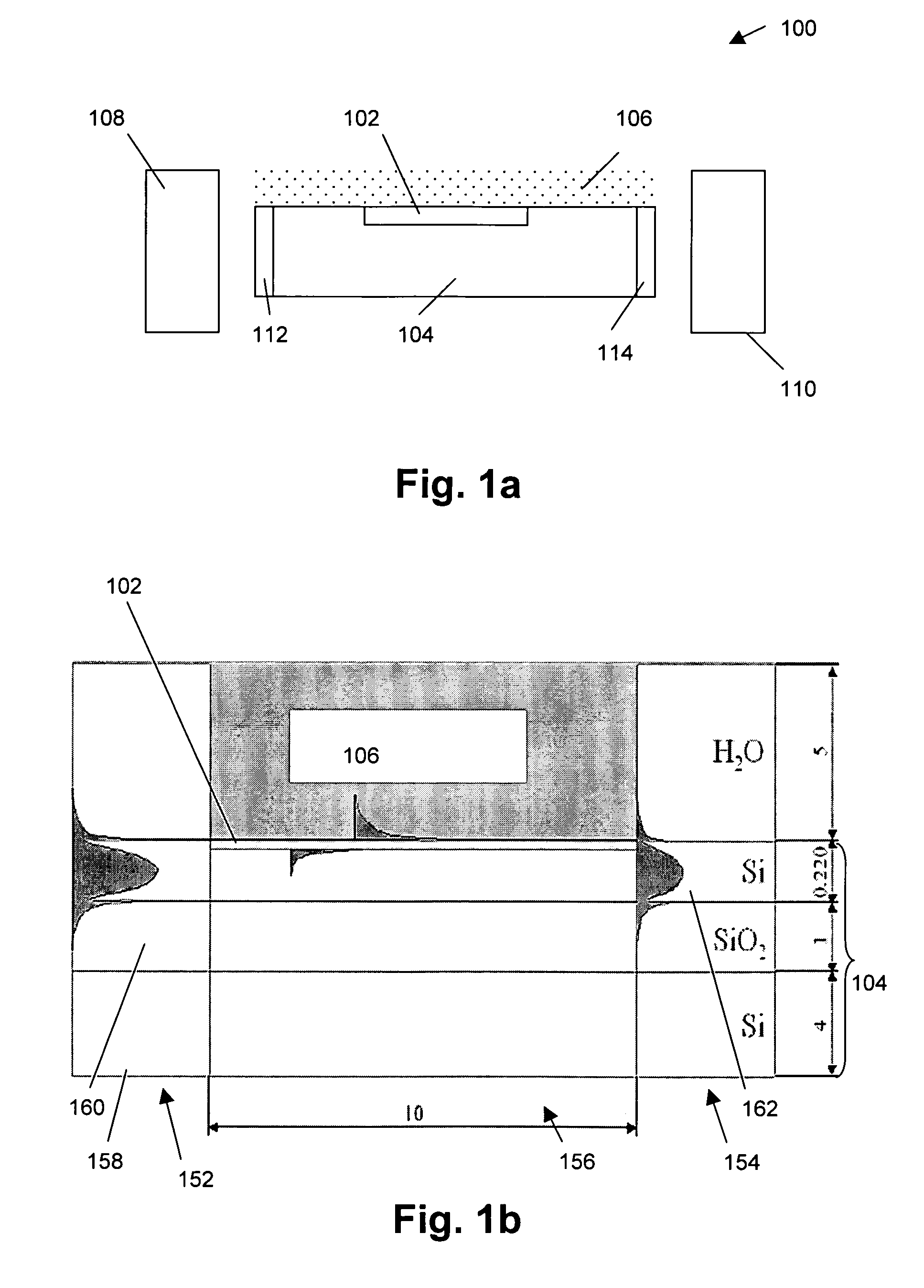
TABLE 1Thickness (μm)MaterialnInput waveguide:substrate4.0Si3.45buried oxide2.0SiO21.45core0.22Si3.45cladding5H2O1.33Sensing waveguide:substrate4.0Si3.45buried oxide2.0SiO21.45core0.135Si3.45metal layer0.060AuFIG. 8a, 8bcladding5H2O1.33length sensing section8.639μm

FIG. 10a illustrates the obtained transmission spectrum through the structure, indicated in dB, as function of the wavelength, indicated in μm. A clear destructive interference peak can be seen in the spectrum around 1550 nm.

example 3

[0085]Example 3 illustrates a simulated result for a system as shown in the second example, whereby the Si core has a thickness of 0.129 μm, the cladding is 5 μm thick and comprises air (refractive index 1) and the length of the sensing section is 13.145 μm. The latter allows to illustrate the effect of changing the length of the sensing section and the cladding material, resulting in a transmission spectrum as shown in FIG. 10b. In other words, the device can be adapted and / or optimised for sensing in a different media. In the present example, the device is adapted for sensing in air media, more than in aqueous environments. The length of the sensing sections used depends on the material system and the refractive index at which the interference minimum is to be detected as is explained above. As a refractive index of 1 is used instead of 1.33 in the previous examples, a different sensing length is applied.


PUM


Abstract

An optical detection system (100) for detecting biological, chemical or bio-chemical particles is described. The optical detection system (100) typically comprises a surface mode interference means. The surface mode interference means may comprise a layer (102) such as for example a metal layer like e.g. a gold layer. The surface mode interference means furthermore typically is adapted to create an interference effect between optical interface modes of the layer to detect optical changes in the vicinity of the layer (102). In this way, sample (106) occurring in the vicinity of the surface may be detected. The present invention furthermore relates to a method for performing optical detection and to a method for setting up an optical detection system wherein parameters are selected for tuning the surface mode interference means to a desired wavelength range and/or to a desired range of analyte refractive indices.

Description

TECHNICAL FIELD OF THE INVENTION[0001]The present invention relates to methods and systems for biological, biochemical or chemical sensing and / or detecting of particles. More particularly, the present invention relates to methods and systems for biological, biochemical and / or chemical sensing and / or detecting of particles using surface mode measurements, like surface plasmon measurements.BACKGROUND OF THE INVENTION[0002]The use of surface plasmon resonance (SPR) for biological and chemical sensing is well established. The high sensitivity of this technique to surface phenomena makes it ideal for use in real-time and label-free biosensors where very small changes in refractive index must be detected. Driven by the vision of a laboratory on a chip and its impact in numerous applications such as detection, bio sensing, kinetic and binding studies and point-of-care diagnostics, extensive work has been done to miniaturize SPR biosensors. In the past decade, several integrated optical SPR...

Claims


Application Information

Patent Timeline
IPC IPC(8): G01N21/55G01N21/01
CPCB82Y20/00G01N21/553G02B6/1226G01N21/7703G01N21/554
Inventor DEBACKERE, PETERSCHEERLINCK, STIJNBAETS, ROELBIENSTMAN, PETER
Owner INTERUNIVERSITAIR MICRO ELECTRONICS CENT (IMEC VZW)
Why Eureka
Try Eureka