Substrate processing apparatus and substrate placing table

A technology of substrate processing device and mounting table, which is applied to gaseous chemical plating, coating, electrical components, etc., can solve the problems of influence of film formation characteristics, low temperature, non-uniformity, etc., so as to improve temperature controllability and restrain temperature rise , to achieve the effect of film forming characteristics

Inactive Publication Date: 2009-02-25
TOKYO ELECTRON LTD
View PDF1 Cites 11 Cited by
  • Summary
  • Abstract
  • Description
  • Claims
  • Application Information

AI Technical Summary

Problems solved by technology

[0007] In general, when the temperature of the peripheral portion of the wafer placed on the stage is lower than the temperature of the central portion, the film formation characteristics will be affected. For example, it was confirmed that the composition of the formed film In-plane unevenness is the cause of poor film formation
Therefore, attempts were made to improve film formation characteristics by controlling the heating temperature of the outer peripheral region of the mounting table, but this did not yield a sufficient improvement effect.
[0008] In addition, in order to improve the film formation characteristics, if the outer peripheral region of the mounting table is heated to increase the temperature, the shower head disposed opposite to the mounting table will become high in temperature due to the radiant heat from the mounting table, and it will be difficult to control the shower head. temperature control
More specifically, the temperature on the outer side becomes higher than that in the central part of the shower head, and the temperature on the outer peripheral part becomes extremely low. The formation of such a temperature distribution naturally affects the film formation characteristics.

Method used


Image

  • Substrate processing apparatus and substrate placing table
  • Substrate processing apparatus and substrate placing table
  • Substrate processing apparatus and substrate placing table

Examples


Embodiment Construction

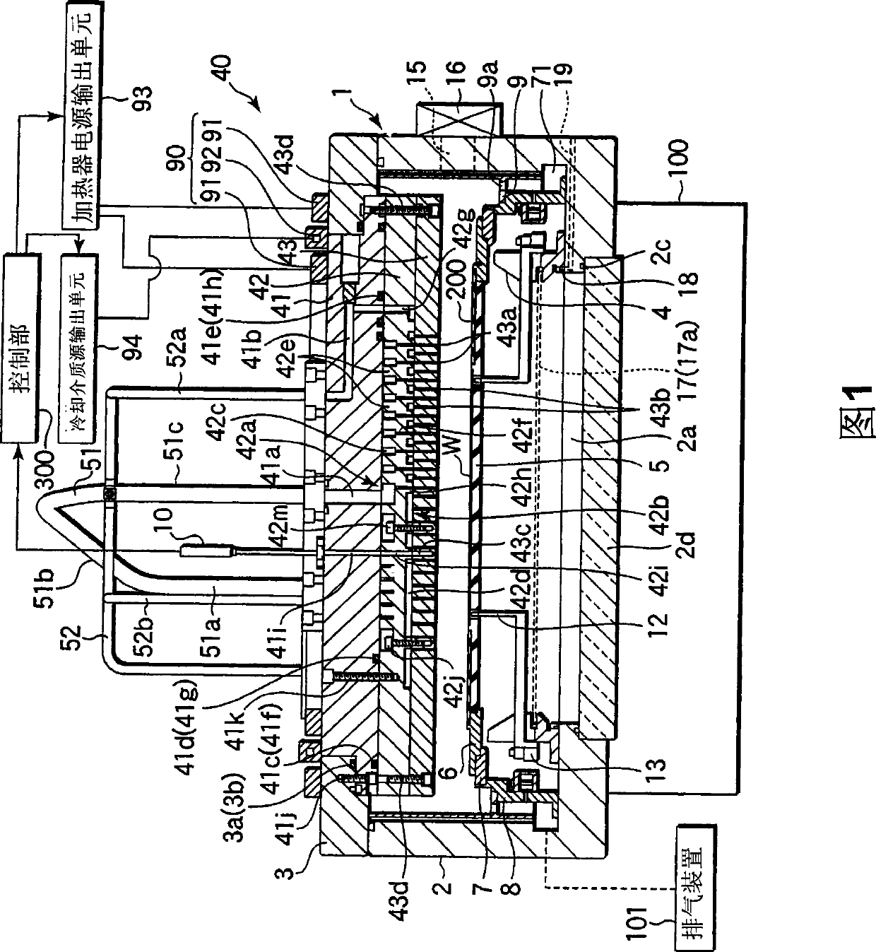
[0052] Hereinafter, preferred embodiments of the present invention will be described with reference to the drawings.

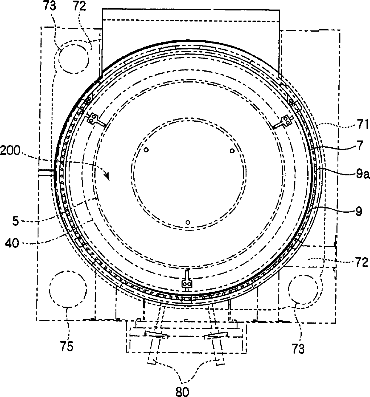
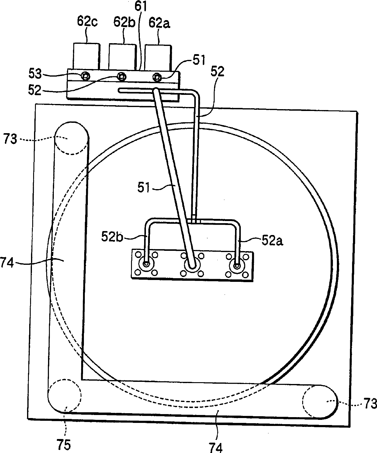
[0053] 1 is a cross-sectional view showing a film forming apparatus according to an embodiment of a substrate processing apparatus of the present invention, figure 2 is a plan view showing the internal structure of the housing of the film forming apparatus, image 3 is its top plan. Figure 4 ˜ FIG. 11 are schematic views showing components of a shower head constituting the film forming apparatus. Among them, in Fig. 1, the cross-section of the shower head represents the Figure 6 The cross section of the line X-X is asymmetrical with respect to the central part.

[0054] As shown in FIG. 1 , the film forming apparatus has a frame 1 made of, for example, aluminum or the like and has a substantially rectangular planar section, and the inside of the frame 1 is a bottomed cylindrical processing container 2 . An opening 2a for connecting the lamp unit 100 is p...


PUM


Abstract

A film forming apparatus is provided with a processing container (2) for storing a semiconductor wafer (W); a substrate placing table (5) arranged inside the processing container (2) for placing the semiconductor wafer (W); a shower head (40) arranged at a position facing the placing table (5) as a processing gas blowing mechanism for blowing out a processing gas into the processing container (2); and an exhauster (101) for exhausting inside the processing container (2). The substrate placing table (5) is provided with a placing table main body (5a), and a heat blocking body (200), which is arranged on the placing table main body (5a) in a region outside a region where the semiconductor wafer (W) is placed, and reduces heat diffusion from the placing table main body to the shower head (40).

Description

technical field [0001] The present invention relates to a substrate processing apparatus for performing processing such as film formation on a substrate to be processed such as a semiconductor wafer, and a substrate mounting table for mounting the substrate to be processed in the substrate processing apparatus. Background technique [0002] In the manufacturing process of semiconductor devices, a thin film composed of various substances is formed on a semiconductor wafer (hereinafter referred to as "wafer") as an object to be processed. The materials and combinations used in the art are also diversified and complicated. [0003] For example, in semiconductor storage elements, in order to overcome the performance limit caused by the refresh (reflash) operation of DRAM (Dynamic Random Access Memory) elements, the use of ferroelectric capacitors has been carried out. The development of dielectric thin films to manufacture high-capacity storage elements. This kind of ferroelec...

Claims


Application Information

Patent Timeline
Patent Type & Authority Applications(China)
IPC IPC(8): C23C16/455C23C16/46H01L21/31H01L21/683
CPCC23C16/45561C23C16/46C23C16/45574C23C16/45565C23C16/4557C23C16/45572C23C16/4585H01L21/68757H01L21/205H01L21/3065H01L21/683
Inventor 饭塚八城
Owner TOKYO ELECTRON LTD
Why Eureka
Try Eureka