Financial tax control SOC chip logic checking system

A logic verification and financial tax technology, applied in the field of logic verification system, can solve the problems of complex verification and testing work, shorten the development cycle and improve the design performance.

Inactive Publication Date: 2009-03-04
LANGCHAO ELECTRONIC INFORMATION IND CO LTD
View PDF0 Cites 6 Cited by
  • Summary
  • Abstract
  • Description
  • Claims
  • Application Information

AI Technical Summary

Problems solved by technology

[0002] With the development of microelectronics technology, the integration of chips is getting higher and higher, and the design and application of SOC chips is becoming more and more common, but its verification and testing work is becoming more and more complicated.

Method used


Image

  • Financial tax control SOC chip logic checking system
  • Financial tax control SOC chip logic checking system
  • Financial tax control SOC chip logic checking system

Examples


Embodiment Construction

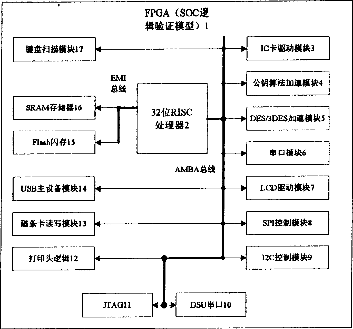
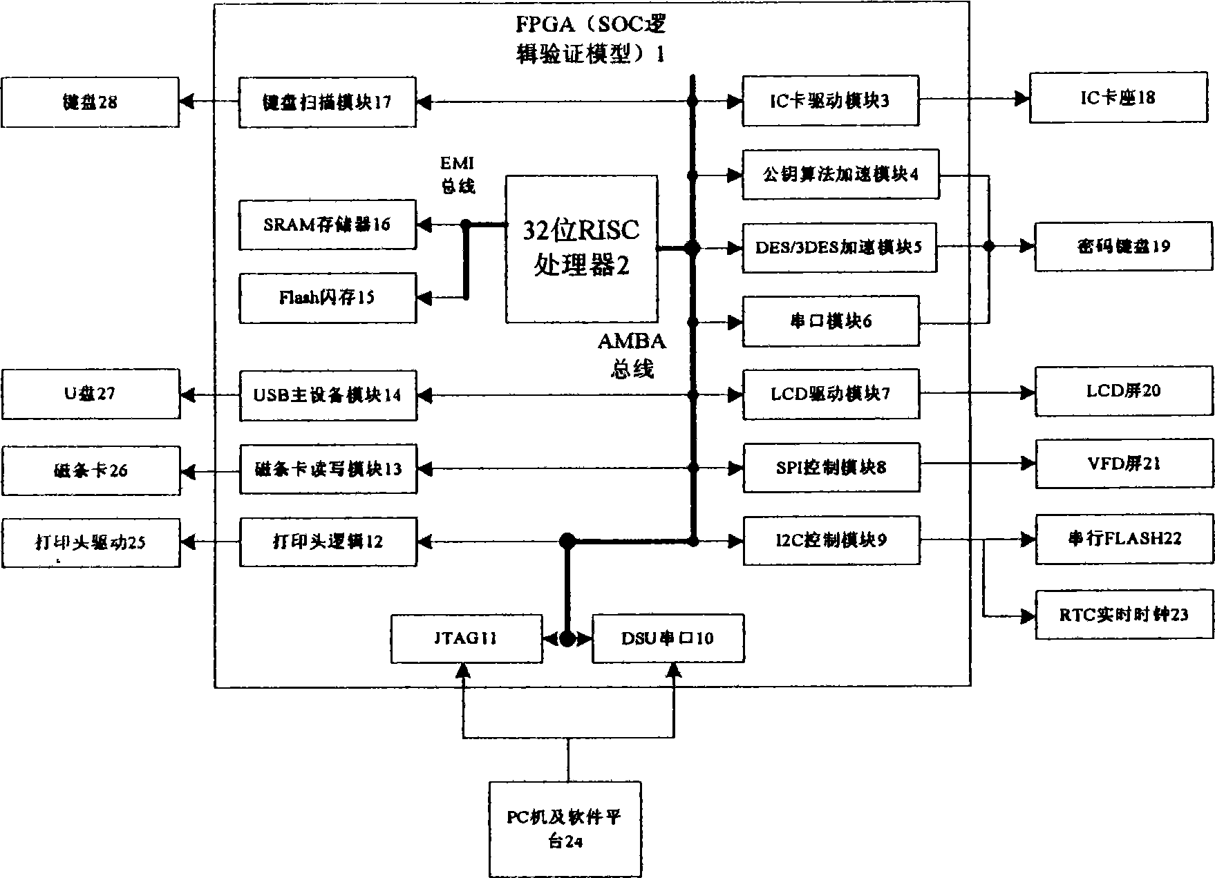
[0015] figure 1 It is a schematic diagram of the SOC logic verification model. Among them, the structure of the SOC logic verification model includes 32-bit RISC processor, IC card driver module 3, public key algorithm acceleration module 4, DES / 3DES acceleration module 5, serial port module 6, LCD driver module 7, SPI control module 8, I2C control module 9, DSU serial port 10, JTAG11, print head logic 12, magnetic stripe card read-write module 13, USB master module 14, Flash flash memory 15, SRAM memory 16 and keyboard scanning module 17, wherein, IC card driver module 3 , public key algorithm acceleration module 4, DES / 3DES acceleration module 5, serial port module 6, LCD driver module 7, SPI control module 8, I2C control module 9, DSU serial port 10, JTAG11, print head logic 12, magnetic stripe card reading and writing Module 13, USB master module 14 and keyboard scanning module 17 are connected to 32-bit RISC processor through AMBA bus, Flash flash memory 15 and SRAM memo...


PUM


Abstract

The invention provides a financial tax control used SOC chip logic verification system. In the SOC chip logic verification system, a field programmable gate array FPGA is used for establishing a financial tax control SOC chip system. The system comprises a software platform and a hardware platform. The hardware platform comprises a chip logic verification model with the FPGA as the carrier of the model, various functional modules and interface modules thereof. The functional modules and the interface modules are connected with the chip logic verification model. The software platform is used for configuration of the chip logic verification model, the functional modules and the interface modules and processing related data, and inputting signals to the interface modules; the incoming signals of the chip logic verification model are generated through each functional module; control signals over software are generated through the chip logic verification model; the signals are converted into software display scalar quantities through each of the functional modules and the interface modules thereof.

Description

technical field [0001] This patent relates to the field of integrated circuit design, specifically a logic verification system for financial and tax control SOC (System On Chip, System On Chip) chips. Background technique [0002] With the development of microelectronics technology, the integration of chips is getting higher and higher, and the design and application of SOC chips is becoming more and more common, but its verification and testing work is becoming more and more complicated. Any chip has to go through a complex process such as algorithm design, system design, RTL design, layout planning and synthesis, layout, wiring, verification, and tape-out, and the verification step is full of all steps. Therefore, it can be said that verification is the most important part of the chip production process. In the past, the logic verification of the chip was mostly through the application-specific integrated circuit ASIC. Because the application-specific integrated circuit ...

Claims


Application Information

Patent Timeline
Patent Type & Authority Applications(China)
IPC IPC(8): G06F17/50
Inventor 于治楼姜凯梁智豪
Owner LANGCHAO ELECTRONIC INFORMATION IND CO LTD
Why Eureka
Try Eureka