White light light-emitting device and manufacturing method thereof

一种发光装置、制作方法的技术,应用在电气元件、电路、半导体器件等方向,能够解决白光颜色不均匀、光程差异大、白光发光二极管应用受限等问题,达到出光颜色均匀的效果

Inactive Publication Date: 2009-03-04
FOXSEMICON INTEGRATED TECHNOLOGY (SHANGHAI) INC +1
View PDF0 Cites 26 Cited by
  • Summary
  • Abstract
  • Description
  • Claims
  • Application Information

AI Technical Summary

Problems solved by technology

Since the side surface of the light-emitting diode chip 64 and its front surface (that is, the upper surface) all emit light, the light intensity of the light emitted from the side and the light emitted from the front are different, and the optical distance of the transparent package body 66 that penetrates the fluorescent substance is different. Larger, it will make the color of the white light converted by the fluorescent substance uneven, resulting in limited application of white light emitting diodes

Method used


Image

  • White light light-emitting device and manufacturing method thereof
  • White light light-emitting device and manufacturing method thereof
  • White light light-emitting device and manufacturing method thereof

Examples


Embodiment Construction

[0014] The embodiments of the present invention will be further described in detail below in conjunction with the accompanying drawings.

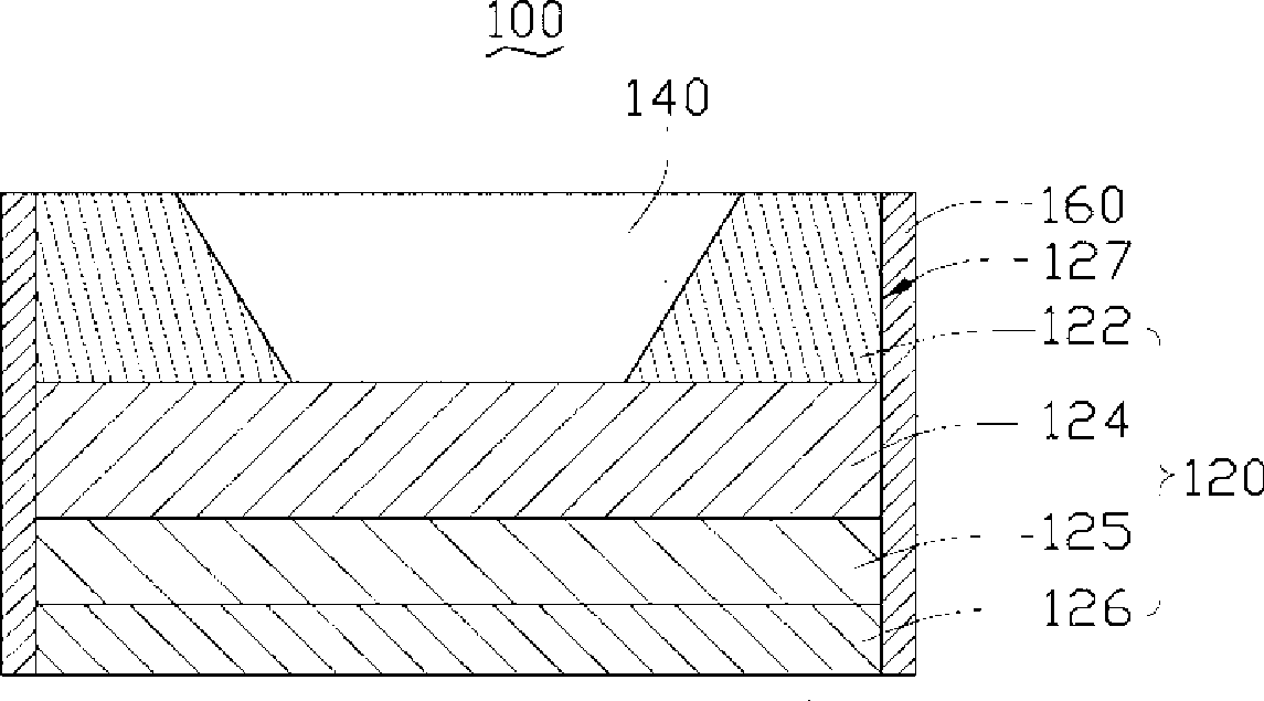
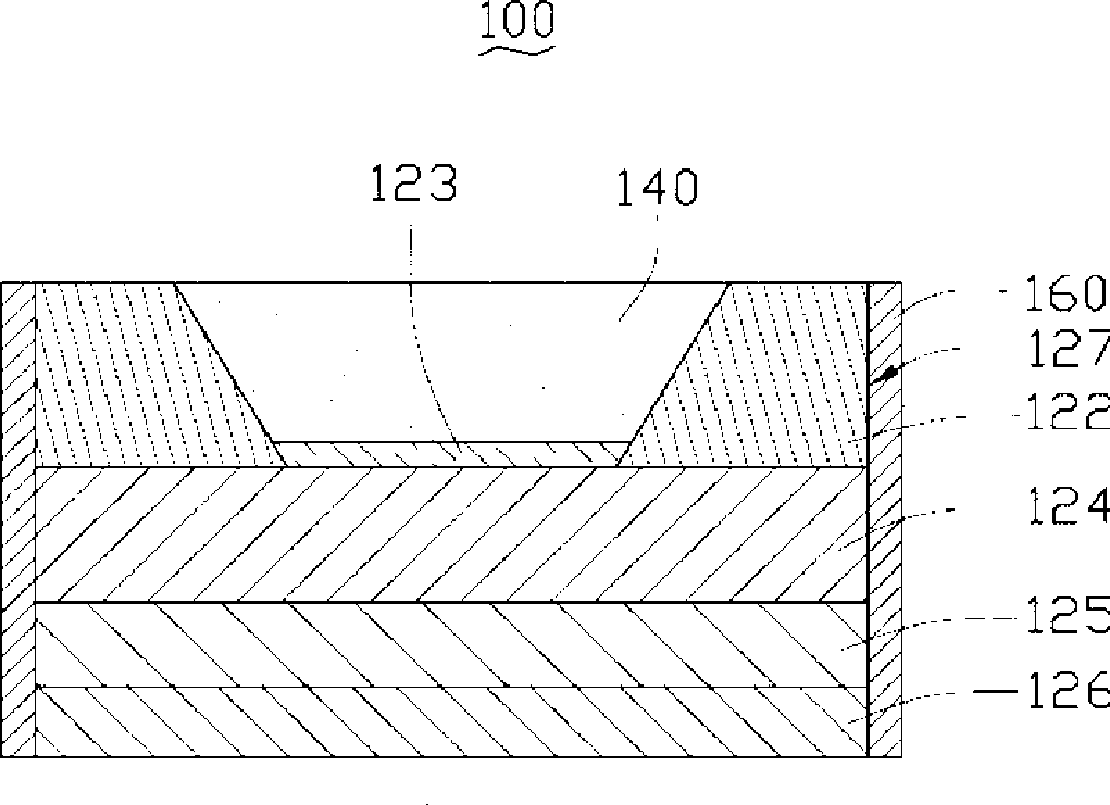
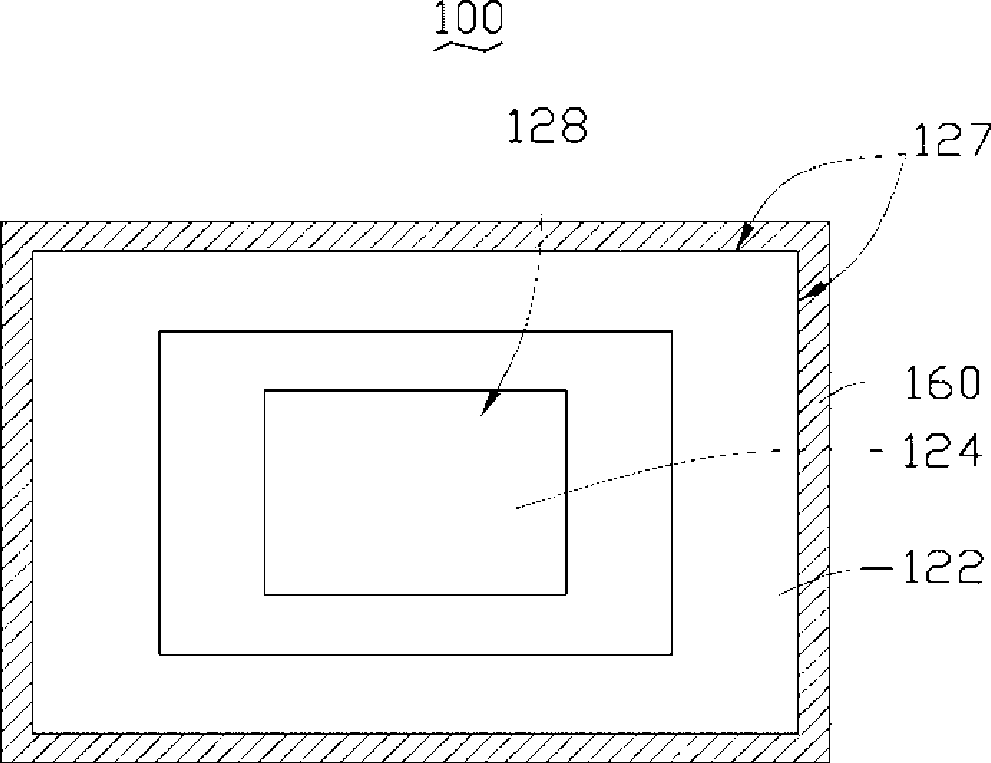
[0015] see Figure 1 to Figure 3 , a white light emitting device 100 provided by an embodiment of the present invention includes a light emitting diode chip 120 , a fluorescent substance layer 140 and a reflective layer 160 .

[0016] The light-emitting diode chip 120 includes a base 122, an n-type semiconductor layer 124, a p-type semiconductor layer 126 having a conductivity type opposite to that of the n-type semiconductor layer 124, and a The active layer 125 in between. The n-type semiconductor layer 124 , the active layer 125 and the p-type semiconductor layer 126 generally form a light emitting structure. The LED chip 120 has a plurality of side surfaces 127 .

[0017] The n-type semiconductor layer 124 , the active layer 125 and the p-type semiconductor layer 126 are disposed on the base 122 and arranged along a direction away fr...


PUM


Abstract

The invention relates to a white light illuminator and a fabrication method thereof. The white light illuminator comprises a light emitting diode chip, a fluorescent material layer and a reflecting layer. The light emitting diode chip comprises a substrate and a luminous structure on the substrate and the luminous structure comprises a first type semiconductor, a second type semiconductor and an active layer between the first and the second type semiconductors. The first type semiconductor, the active layer and the second type conductor are arranged along a direction away from the substrate; at least one groove is formed on the substrate so as to lead part of the first type semiconductor to be exposed; the light emitting diode chip is provided with a plurality of sides; and the fluorescent material layer is arranged in at least one groove of the substrate of the light emitting diode chip, and used for wavelength conversion so as to form white light. The reflecting layer is formed on the sides of the light emitting diode chip to surround the light emitting diode chip. As the white light illuminator adopts the design of the reflecting layer and fluorescent material layer, the emitted color of the light is uniform.

Description

technical field [0001] The invention relates to the field of semiconductor light emitting, in particular to a white light emitting device and a manufacturing method thereof. Background technique [0002] Currently, white light emitting diode (White Light Emitting Diode, White LED), as a white light emitting device, is widely used as LCD display backlight and vehicle light source because of its low power consumption, long life, small size and high brightness. and general lighting sources, for details, please refer to the article "Unique White LED Packaging Systems" published by Atsushi Okuno et al. at the 2003 IEEE Electronic Components and Technology Conference. [0003] Such as Figure 6 As shown, a typical white light emitting diode 60 includes a base 62 , a light emitting diode chip 64 and a transparent package 66 doped with fluorescent substances. The LED chip 64 is hermetically packaged by the base 62 and the transparent package 66 . Since the side surface of the ligh...

Claims


Application Information

Patent Timeline
Patent Type & Authority Applications(China)
IPC IPC(8): H01L33/00H01L33/20H01L33/50
CPCH01L33/20H01L33/508H01L33/0079H01L33/007H01L33/0093
Inventor 赖志铭
Owner FOXSEMICON INTEGRATED TECHNOLOGY (SHANGHAI) INC
Why Eureka
Try Eureka