
Pixel, pixel module and liquid-crystal display panel

A liquid crystal display panel, pixel technology, applied in static indicators, nonlinear optics, instruments, etc., can solve problems such as difficult to drive pixels, and achieve the effect of reducing the total number of source/gate channels and reducing requirements

Inactive Publication Date: 2009-03-25
BEIJING BOE OPTOELECTRONCIS TECH CO LTD
View PDF0 Cites 37 Cited by
  • Summary
  • Abstract
  • Description
  • Claims
  • Application Information

AI Technical Summary

Problems solved by technology

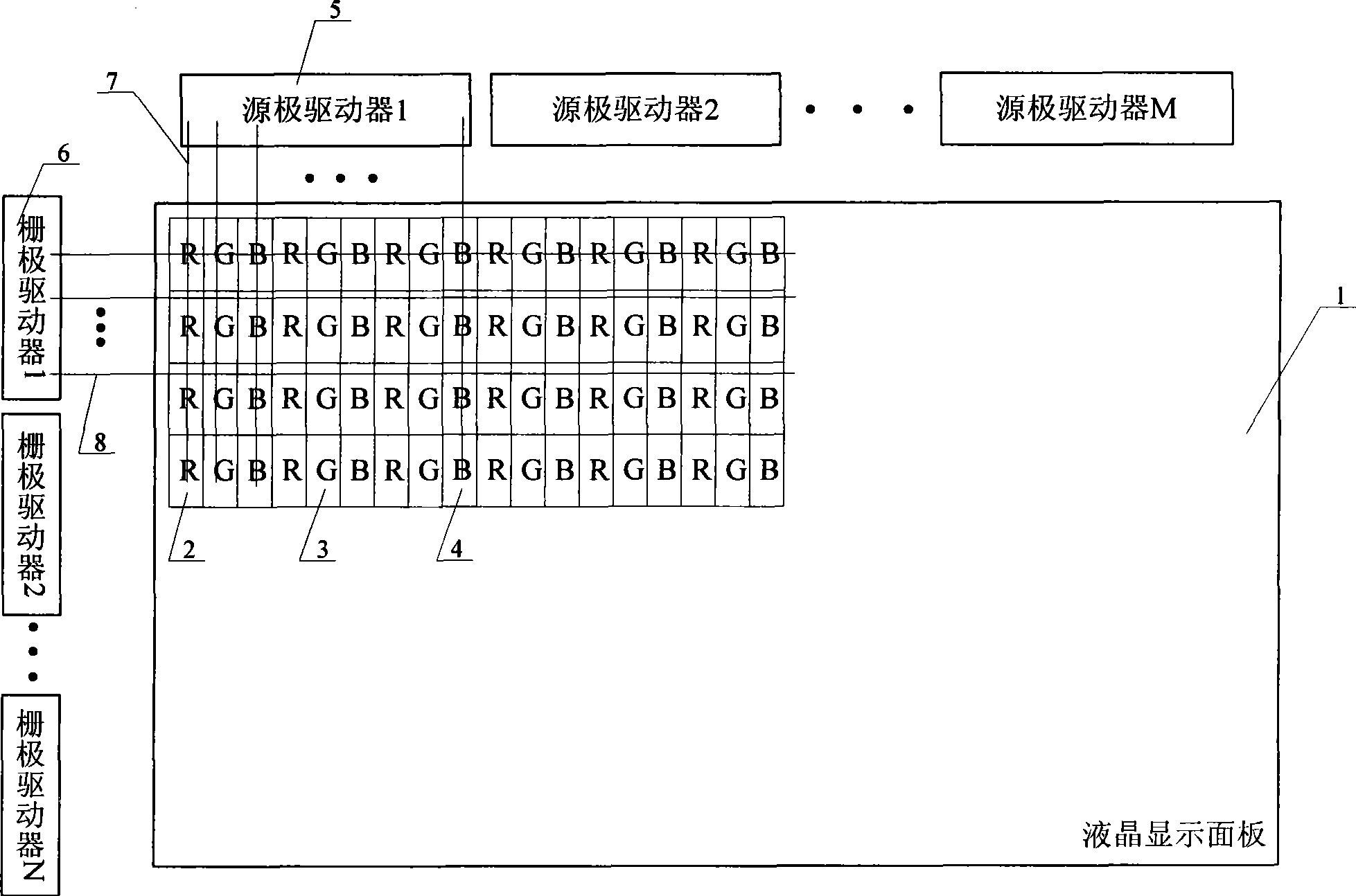
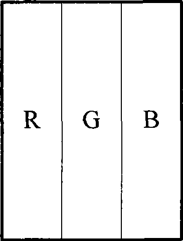
In addition, the number of sub-pixels that need to be driven by a single source channel will be increased by 3 times. With the driving capability of the existing source driver, it is difficult to drive so many pixels.

Method used


Image

  • Pixel, pixel module and liquid-crystal display panel
  • Pixel, pixel module and liquid-crystal display panel
  • Pixel, pixel module and liquid-crystal display panel

Examples


Embodiment 1

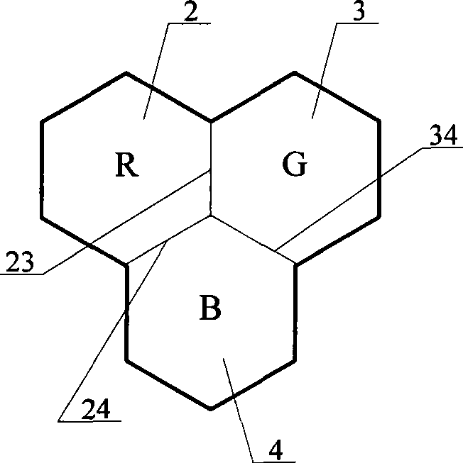
[0028] Such as Figure 3A Shown is the arrangement structure of multiple pixels on the liquid crystal display panel in this embodiment. The central connection lines of the three sub-pixels are arranged in an equilateral triangle. There is no pixel of the same color as the pixel among the six adjacent sub-pixels around the pixel. Such as Figure 3A As shown in , the six sub-pixels adjacent to each side of the sub-pixel R2′ are respectively arranged at intervals of G sub-pixels and B sub-pixels; for the sub-pixels at the edge of the liquid crystal display panel 1, such as R 2", the two sides of which are not shown adjacent to the sub-pixel are respectively adjacent to the G sub-pixel 101 and the B sub-pixel 102 corresponding to the bottom side. Figure 3A The first row where the pixels 9 and 10 are located, the second row where the pixels 11 and 12 are located, and so on, the pixels of the honeycomb distribution are arranged in a 6 (column) × 4 (row) dot matrix; Figure 3B Th...

Embodiment 2

[0030] In the embodiment of the present invention, the direction in which the central lines of sub-pixels are connected in a straight line is the horizontal direction of the pixel module, such as Figure 4A Middle gate channel 8 is connected to the pixel direction or Figure 4B The middle source channel 7 is connected to the pixel direction; the direction in which the center line of the sub-pixel is zigzag connected is the longitudinal direction of the pixel module, such as Figure 4A The source channel 7 is connected in the pixel direction or as Figure 4B The middle gate channel 8 is connected to the pixel direction.

[0031] Such as Figure 4AAs shown, the pixel modules adopt the arrangement described in the above-mentioned embodiment 1, and it is defined that the central connection line of the sub-pixel is connected in a straight line as the horizontal direction of the pixel module, such as the direction of the gate channel 8 connecting the pixel; the central connection ...

Embodiment 3

[0033] Such as Figure 4B As shown, the pixel module adopts the arrangement described in the above-mentioned embodiment 1, and defines that the center line of the sub-pixel is connected in a straight line as the horizontal direction of the pixel module, such as the source channel 7 connecting the pixel direction; the center line of the sub-pixel is in the direction of The zigzag connection is the longitudinal direction of the pixel module, for example, the gate channel 8 is connected to the pixel direction. Horizontally, the sub-pixels whose center line is on the same straight line share one source channel 7; vertically, each of the sub-pixels on the same lateral edge shares one gate channel 8, except for the edges, the sub-pixels Connected in sequence, the sub-pixels on each connection share a gate channel 8, and connected in sequence: the center connection of the sub-pixel is the same shape as the center connection of the sub-pixels on both sides of the edge, such as Figur...


PUM


Abstract

The present invention provides a pixel, a pixel module and a liquid crystal display panel. The liquid crystal display panel consists of the pixel modules which are in honeycomb-shaped arrangement. The pixel module consists of a red sub-pixel, a green sub-pixel and a blue sub-pixel which are of regular hexagon shapes respectively. All sub-pixels in the pixels are in honeycomb-shaped arrangement. Each sub-pixel is different in color from six adjacent sub-pixels. A unique pixel structure and a unique pixel module structure are provided and the liquid crystal display panel is provided based on the special structures. The number of the source electrode drive channels required by the pixels on the panel is reduced, and the increased number of the required grid electrode drive channels is reduced as possible so that the number of the required source / grid electrode drive channels is minimized and the cost of the liquid crystal display panel is reduced.

Description

technical field [0001] The invention relates to a pixel, a pixel module and a liquid crystal display panel, in particular to a pixel, a pixel module and a liquid crystal display panel composed of three sub-pixels including red, green and blue. Background technique [0002] In recent years, attention has been paid to liquid crystal display devices characterized by thinness and low power consumption, and such liquid crystal display devices are generally classified into active type and passive type. However, the active type is superior in terms of large size and high definition. Generally, active elements in liquid crystal display panels use thin film transistors (Thin Film Transistor, hereinafter referred to as TFT) in many cases. [0003] In an active liquid crystal display device (hereinafter referred to as a liquid crystal display device), the active elements and pixels are in a matrix. By driving each active element, a predetermined voltage can be applied to the pixels, t...

Claims


Application Information

Patent Timeline
IPC IPC(8): G02F1/1362G02F1/133G09G3/36
Inventor 丁悦
Owner BEIJING BOE OPTOELECTRONCIS TECH CO LTD
Learn More