Method for controlling sheet resistance of poly in fabrication of semiconductor device

A manufacturing process, sheet resistance technology, applied in semiconductor/solid-state device manufacturing, semiconductor/solid-state device testing/measurement, circuits, etc., and can solve problems such as resistance differences

Inactive Publication Date: 2009-03-25
DONGBU HITEK CO LTD
View PDF1 Cites 0 Cited by
  • Summary
  • Abstract
  • Description
  • Claims
  • Application Information

AI Technical Summary

Problems solved by technology

That is, in the case where the LDD dummy layer is generated by using the MDP generation rule in order to satisfy the sheet resistance of the polysilicon resistor, the LDD ion implantation is not performed in the polysilicon region where the LDD dummy layer is generated, resulting in a significant loss in resistance. difference

Method used


Image

  • Method for controlling sheet resistance of poly in fabrication of semiconductor device
  • Method for controlling sheet resistance of poly in fabrication of semiconductor device
  • Method for controlling sheet resistance of poly in fabrication of semiconductor device

Examples


Embodiment Construction

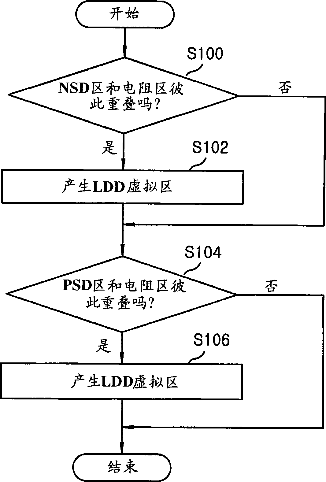
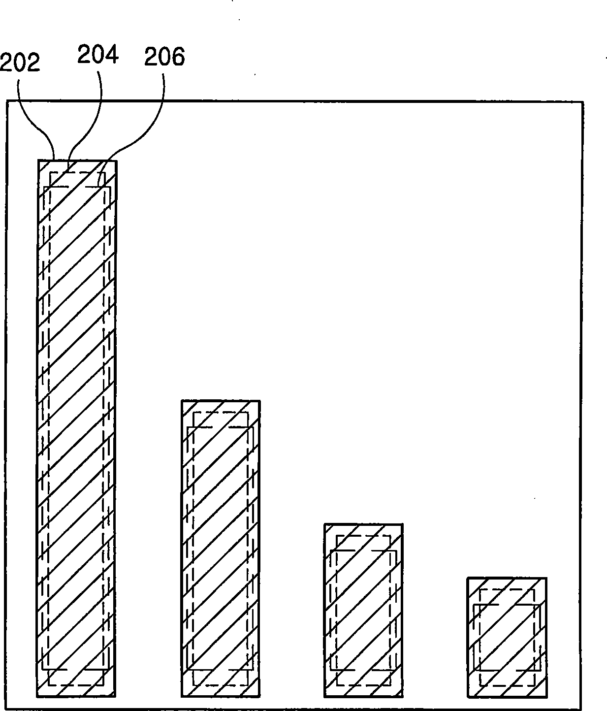
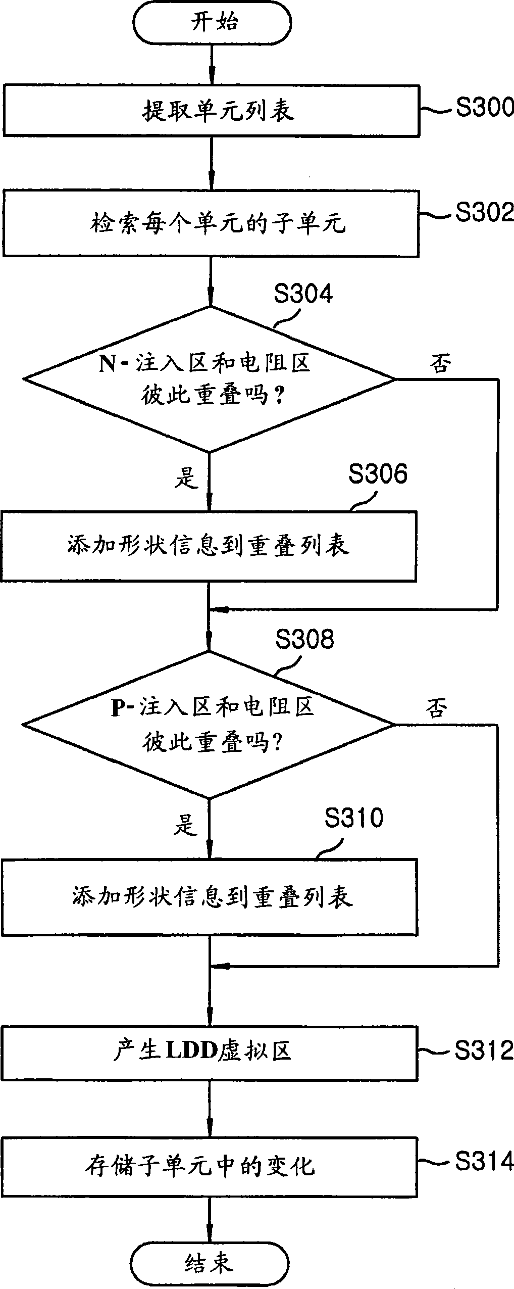
[0017] In the following detailed description of the embodiments, reference will now be made in detail to certain specific embodiments of the invention and to the embodiments illustrated in the accompanying drawings. Wherever possible, the same symbols will be used throughout the drawings to refer to the same or like parts. These specific embodiments are described in sufficient detail to enable those skilled in the art to practice the invention. Other embodiments may be utilized and structural, logical, electrical changes may be made without departing from the scope of the present invention. Moreover, it can be understood that various specific embodiments of the present invention, although different, are not necessarily independent of each other. For example, a distinctive feature, structure or characteristic described in one embodiment may also be included in other embodiments. Therefore, the following detailed description should not be interpreted as limiting, but the scope...


PUM


Abstract

A method for controlling the sheet resistance of poly in the fabrication of a semiconductor device. In one example embodiment, a method for controlling the sheet resistance of a poly in the fabrication of a semiconductor device includes various steps. First, detection is made whether or not an N-ion implantation area and a resistance area overlap with each other within the layout of a cell to be formed on a semiconductor wafer. Next, an LDD dummy area is generated in the area on the layout where the N-ion implantation area exists if such overlap is found. Then, detection is made whether or not a P-ion implantation area and a resistance area overlap with each other within the layout. Finally, an LDD dummy area is generated in the area on the layout where the P-ion implantation area exists if such overlap is found.

Description

[0001] This application claims priority from Korean Patent Application No. 10-2007-0095272 filed on September 19, 2007, the entire contents of which are hereby incorporated by reference. technical field [0002] Embodiments of the present invention relate to a method of manufacturing a semiconductor device, and more particularly, to a method of precisely controlling sheet resistance of a non-salicide. Background technique [0003] Typically, in order to reduce the hot carrier effect by relatively reducing the small electrical field, a lightly doped drain (LDD) structure is used. For example, an LDD structure may be used in a 130nm process. In the LDD structure, the LDD dummy layer controls the sheet resistance of polysilicon by allowing LDD ion implantation on the polysilicon pattern after the resistive pattern is formed. [0004] In order to determine whether LDD ion implantation has actually been performed, a test may be performed by drawing an LDD dummy layer in a scribe...

Claims


Application Information

Patent Timeline
Patent Type & Authority Applications(China)
IPC IPC(8): H01L21/00H01L21/66
CPCH01L22/14H01L22/00H01L21/18
Inventor 崔兰顺
Owner DONGBU HITEK CO LTD
Why Eureka
Try Eureka