Fabrication method for surface silver electrode of silicon based organic light emitting micro display device

A technology of micro-display devices and silver electrodes, which is applied in semiconductor/solid-state device manufacturing, semiconductor devices, electric solid-state devices, etc., can solve problems such as surface electrode unevenness, and achieve the effect of improving adhesion and not easy to fall off

Inactive Publication Date: 2009-03-25
INST OF MICROELECTRONICS CHINESE ACAD OF SCI
View PDF0 Cites 14 Cited by
  • Summary
  • Abstract
  • Description
  • Claims
  • Application Information

AI Technical Summary

Problems solved by technology

[0004] In order to solve the problem of uneven surface electrodes of organic light-emitting micro-display devices in the prior art, the present invention provides a method for preparing silver electrodes on the surface of silicon-based organic light-emitting micro-display devices, so that the surface electrodes meet the requirements for growing organic light-emitting layers

Method used


Image

  • Fabrication method for surface silver electrode of silicon based organic light emitting micro display device
  • Fabrication method for surface silver electrode of silicon based organic light emitting micro display device
  • Fabrication method for surface silver electrode of silicon based organic light emitting micro display device

Examples


Embodiment Construction

[0032] In order to make the object, technical solution and advantages of the present invention clearer, the present invention will be described in further detail below in conjunction with specific embodiments and with reference to the accompanying drawings.

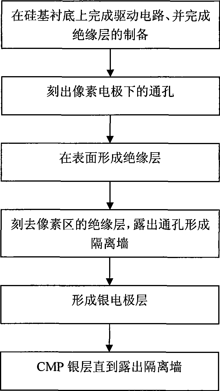
[0033] Such as image 3 as shown, image 3 It is a step diagram of a method for preparing a silver electrode on the surface of a silicon-based organic light-emitting microdisplay device provided by the present invention. The preparation method includes the following steps:

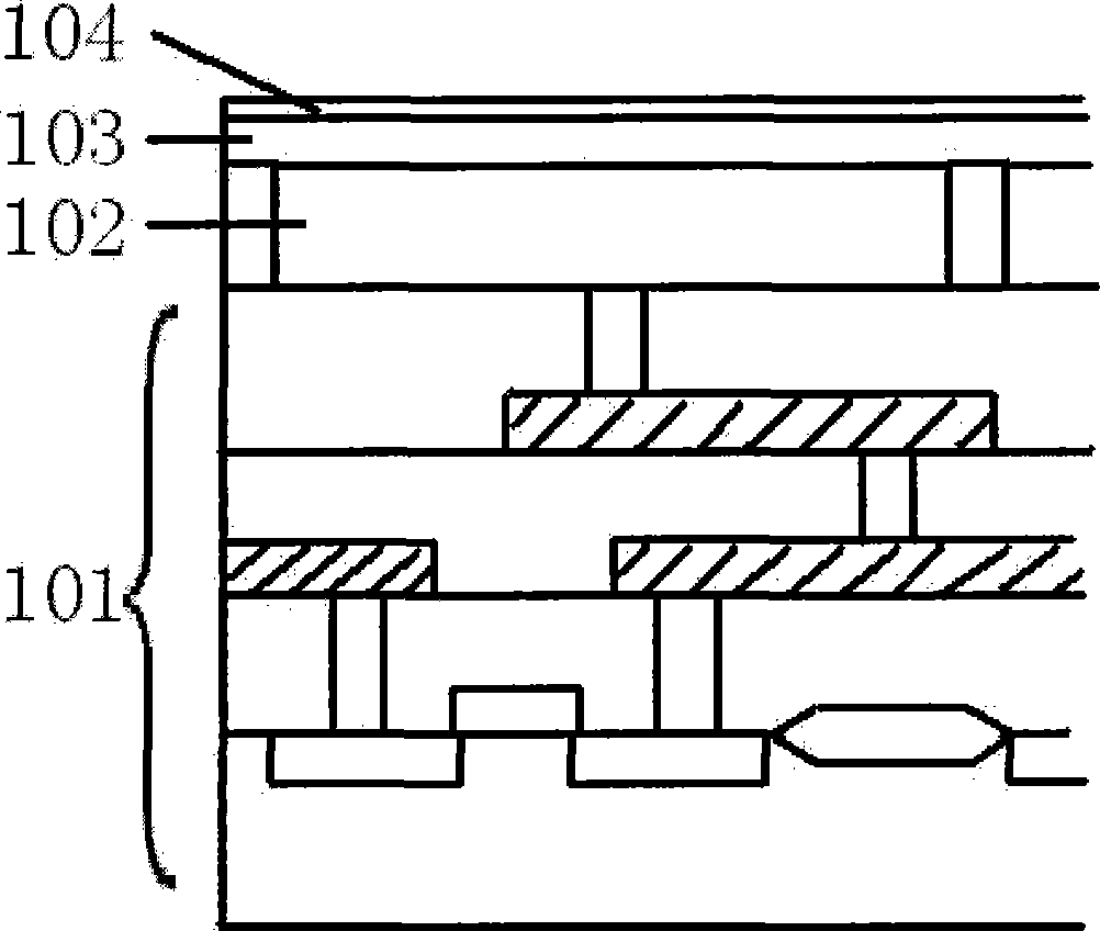
[0034] (1) Complete the driving circuit on the silicon-based substrate and complete the preparation of the insulating layer;

[0035] (2) completing the etching of the through hole under the pixel electrode on the insulating layer;

[0036] (3) growing a layer of insulating layer after completing the through hole;

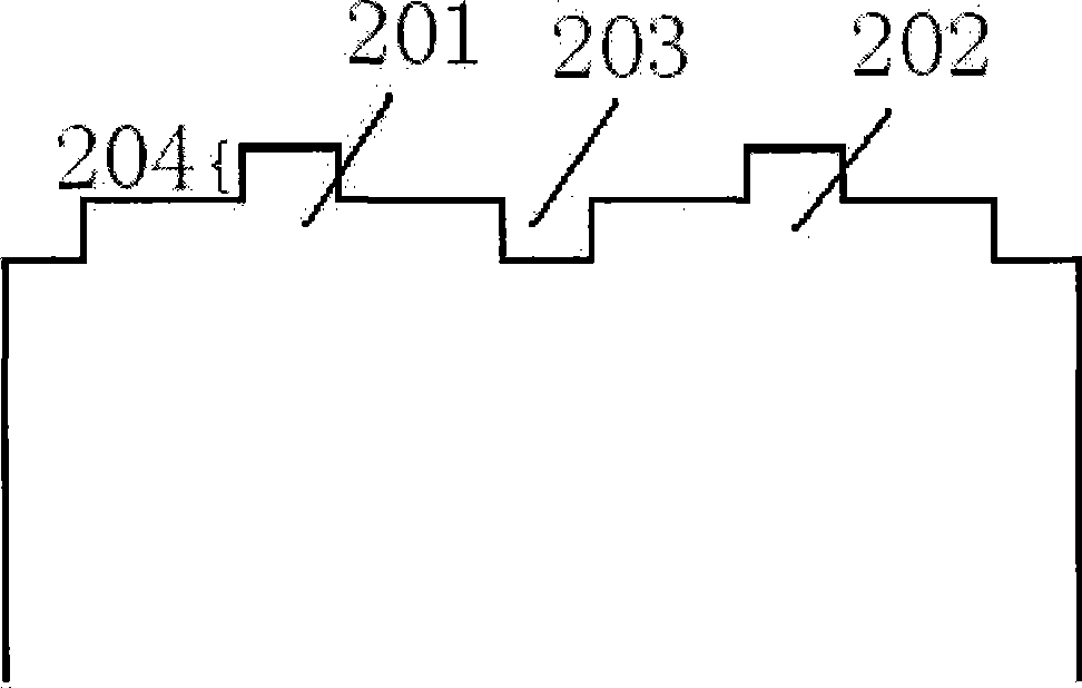
[0037] (4) Etching the insulating layer after photolithography to expose the surface of the pixel area, leaving the insulating layer b...


PUM

PropertyMeasurementUnit
heightaaaaaaaaaa
thicknessaaaaaaaaaa
thicknessaaaaaaaaaa

Abstract

The invention relates to the technical field of manufacturing a silicon-based organic light emitting micro-display device, in particular to a method for preparing silver electrodes on the surface of the silicon-based organic light emitting micro-display device. In order to solve the problem in the prior art that the electrodes on the surface of the silicon-based organic light emitting micro-display device are uneven, the invention provides the method for preparing the silver electrodes on the surface of the silicon-based organic light emitting micro-display device. The method comprises the following steps: drilling through-holes below an internal drive circuit, an insulating layer, and the electrodes arranged on the pixel surface on the substratum of a silicon substrate in sequence; forming an insulating layer on the whole surface; etching after lithography so as to remove the insulating layer from the pixel area with the exposure of the through-holes; preserving insulating layers among pixels as an insulating wall for insulating; then forming a metallic silver layer on the surface; and performing the CMP technology until the insulating wall appears with the pixels isolated from each other. The invention is effective in enabling silver to be more adhesive to the insulating layer with silver not intending to fall out in the cause of performing the CMP technology; and the CMP technology provided by the invention can improve the flatness of the surface, on which the silver electrodes form a damascene-structure.

Description

technical field [0001] The invention relates to the technical field of manufacturing silicon-based organic light-emitting micro-display devices, in particular to a method for preparing a silver electrode on the surface of a silicon-based organic light-emitting micro-display device. Background technique [0002] The micro-display system is a flat panel display technology, its core is to integrate all the pixels for displaying TV images or computer images into an integrated circuit, and the usual size is less than 3in (7.62cm) diagonally. Silicon-based organic light-emitting technology is a realization of micro-display technology, and its basic structure is to grow organic light-emitting diode devices on CMOS silicon chips. Silicon-based organic light-emitting microdisplay chip structure such as figure 1 As shown, the bottom layer is the driving circuit 101, and the present invention does not involve the driving circuit, so this layer will not be described again. The pixel e...

Claims


Application Information

Patent Timeline
Patent Type & Authority Applications(China)
IPC IPC(8): H01L21/822H01L21/28H01L27/32
Inventor 黄苒夏洋杜寰赵毅王晓慧韩郑生潘国顺
Owner INST OF MICROELECTRONICS CHINESE ACAD OF SCI
Why Eureka
Try Eureka