Silicon chip product defect analysis method and device

A defect analysis and silicon wafer technology, applied in measurement devices, analysis materials, material analysis by optical means, etc., can solve the problems of high level requirements, untimely response, low production efficiency, etc., to ensure repeatability and comparability performance, saving storage space, and high accuracy

Active Publication Date: 2011-02-02
SHANGHAI HUAHONG GRACE SEMICON MFG CORP
View PDF0 Cites 2 Cited by
  • Summary
  • Abstract
  • Description
  • Claims
  • Application Information

AI Technical Summary

Problems solved by technology

[0003] However, this traditional defect analysis method has the following disadvantages: firstly, it does not respond to abnormal defects in time. After a period of time after the production process of silicon wafer products, it starts to analyze the defects of silicon wafer products. Defects caused by abnormal production equipment cannot be reflected in time; secondly, in this defect analysis method, the defect analysis equipment can only analyze one silicon wafer at a time, and the production efficiency is low. For large-scale production line silicon wafer products, only Sampling surveys cannot fully reflect the abnormalities of silicon wafer products; since standard graphics must be made first, the standard file production level is relatively high, and a large number of standard files need to be retained on the hardware of the defect analysis equipment. higher volume requirements

Method used


Image

  • Silicon chip product defect analysis method and device
  • Silicon chip product defect analysis method and device
  • Silicon chip product defect analysis method and device

Examples


Embodiment Construction

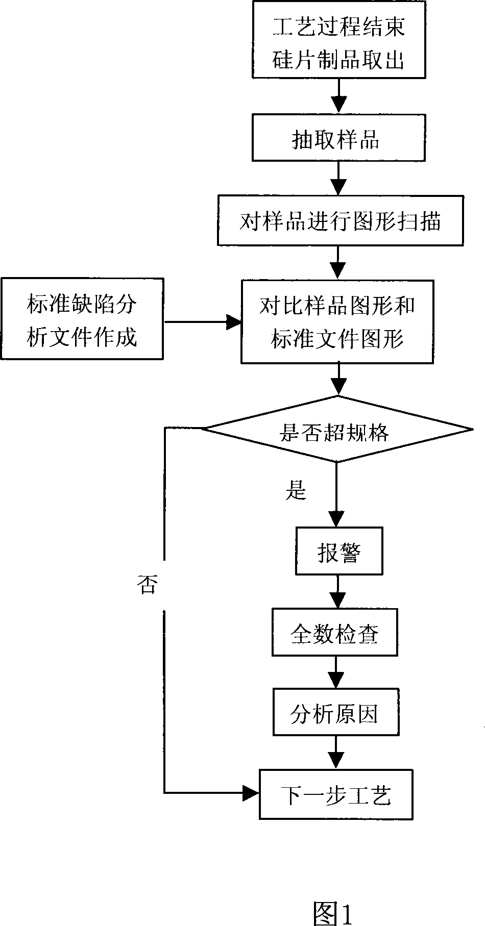
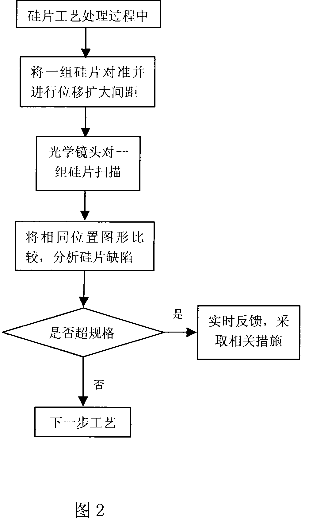
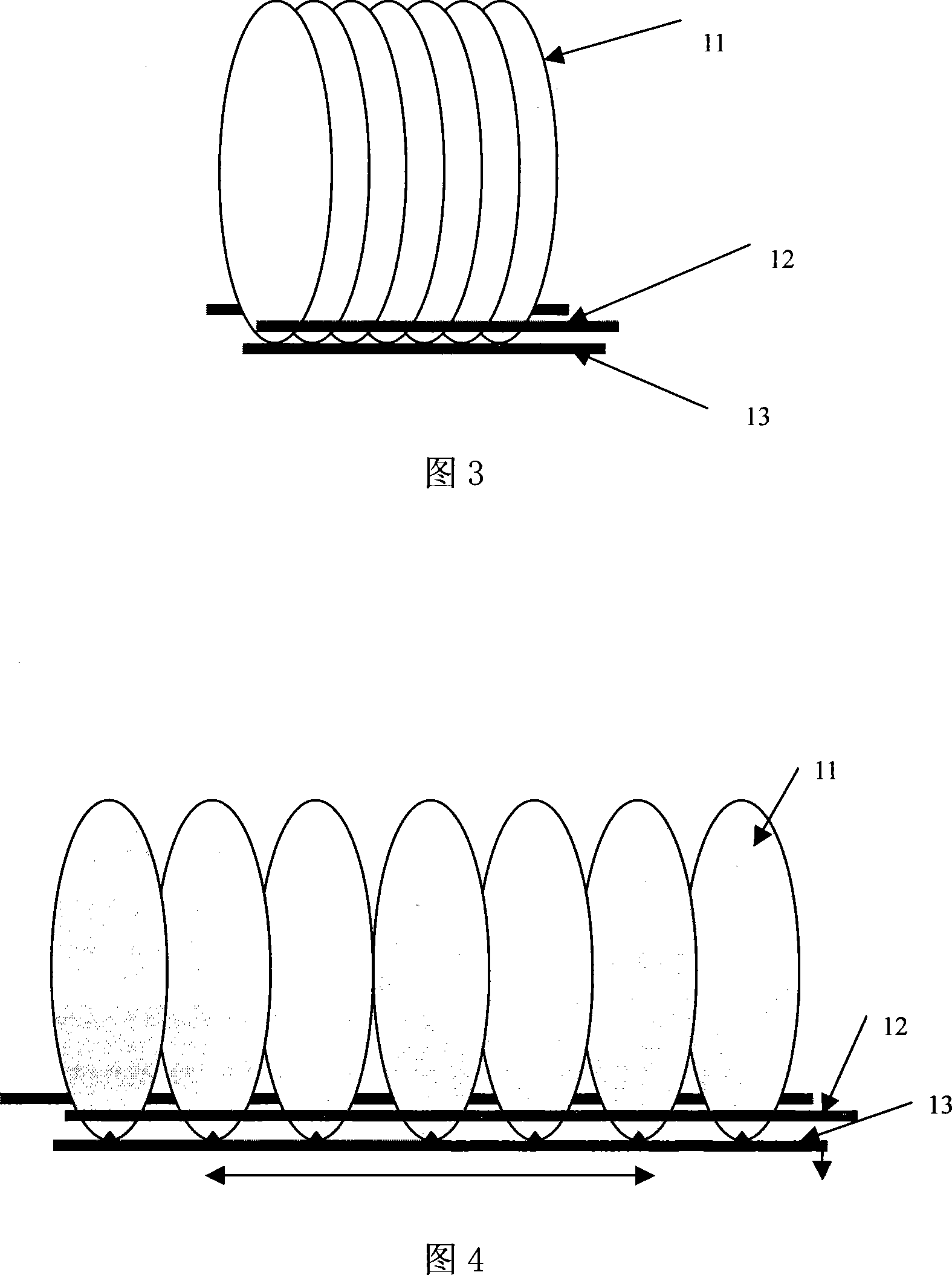
[0021] One embodiment of the defect analysis method for silicon wafer products of the present invention is as follows: figure 2 As shown, in the manufacturing process of silicon wafer products, the graphics at the same position of a batch of silicon wafer products should be the same, and a group of identical silicon wafer products (such as 3 to 25 pieces) are placed on the silicon wafer displacement device, Correspond to the same position of the same group of silicon wafer products, and adjust the distance between each silicon wafer product, so that a set of scanning lenses is placed between the group of silicon wafer products, and at the same time, the same position of the same group of silicon wafer products Scan the graphics, and then use special defect analysis equipment to compare the graphics scanned at the same position of the same group of silicon wafer products to find deviations and abnormalities in the graphics, that is, to find a certain silicon wafer in the group ...


PUM


Abstract

The invention discloses a silicon product defect analysis method which is used for carrying out defect analysis for a plurality of identical silicon products; the method comprises the steps as follows: firstly, positions of one group of identical silicon products for detect analysis are adjusted; subsequently, the images of the same positions of the group of silicon products are scanned; the scanned images of the same positions of the group of the silicon products are compared and analyzed to identify the abnormality of the images; finally, according to the abnormality degree of the image of a certain silicon product, the defect situation of the silicon product is determined; the invention also discloses a silicon product defect analysis device which comprises a silicon sheet displacementdevice, a group of scanning lenses, a stepping motor and an image comparison and recognition system; the invention also discloses another silicon product defect analysis method which is used for carrying out defect analysis for the silicon products with repeated pattern elements. The method and the device can be used for carrying out defect analysis for large batches of silicon products.

Description

technical field [0001] The invention belongs to the field of semiconductor manufacturing, and relates to silicon wafer detection technology, in particular to a silicon wafer product defect analysis method and device. Background technique [0002] Silicon wafer defect analysis methods commonly used in semiconductor production lines are as follows: figure 1 As shown, after the silicon wafer product is taken out at the end of the process, the sample is taken, and the sample silicon wafer product is scanned one by one by using the special defect analysis equipment according to the pre-made standard defect analysis file, and the scanned graphics are compared with the standard defect analysis file. Defect analysis files are compared against standard patterns to identify wafer defects. If there are no defects in the silicon wafer products and do not exceed the specifications, proceed to the next step of the process; if there are defects in the silicon wafer products and exceed the...

Claims


Application Information

Patent Timeline
Patent Type & Authority Patents(China)
IPC IPC(8): G01N21/956H01L21/66
Inventor 张擎雪伍强
Owner SHANGHAI HUAHONG GRACE SEMICON MFG CORP
Why Eureka
Try Eureka