

Mushroom array type surface enhanced Raman spectrum active substrate and preparation method thereof
A surface-enhanced Raman and active substrate technology, which is applied in Raman scattering, nanotechnology for materials and surface science, nano-optics, etc. Guaranteed repeatability, enhanced enhancement, reduced spacing
- Summary
- Abstract
- Description
- Claims
- Application Information
AI Technical Summary
Problems solved by technology
Method used
Image

Examples
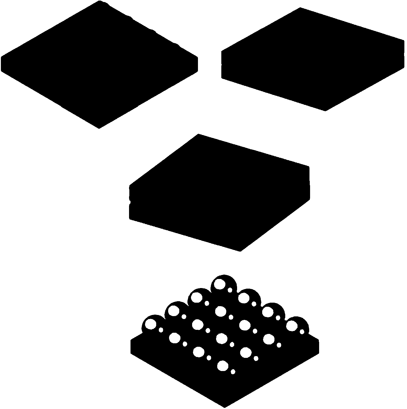
Embodiment 1
[0033] Using electron beam evaporation technology, a gold film with a thickness of 200 nm was deposited on the surface of a two-inch diameter circular silicon wafer after standard cleaning. Standard cleaning steps: 1. Prepare H 2 SO 4 :H 2 O 2 = 1:4 solution, put silicon wafers on a quartz boat, and cook for 15 minutes. Wash with hot deionized water, then change to cold deionized water for cleaning. 2. Place the wafer in HF solution (HF:H 2 Soak in O=1:1) for 30 seconds, take out and rinse with deionized water for 15 minutes. 3. With solution (NH 4 OH: H 2 O 2 :H 2 O=1:1:5) Boil cleaning: first heat the deionized water in the beaker to 85℃, pour the corresponding proportion of NH 4 OH and H 2 O 2 solution, boil for 15 minutes, take out and wash with hot deionized water, then change to cold deionized water for washing. 4. Place the wafer in a diluted HF solution (HF:H 2 O=1:20) for 20 seconds, and then rinse with hot deionized water for 15 minutes. 5. Use solutio...
Embodiment 2
[0036] The composite nano-imprint technology was used to imprint an ordered nano-pore-like structure pattern on the surface of the gold film. The diameter of the nano-pore structure was 200 nm and its period was 400 nm:
[0037]Using the Obducat Eitre6 type nanoimprinting system, firstly using hot imprinting technology, with a two-inch nickel template with a nanopore diameter of 200 nm and a period of 400 nm as the master, the surface nanostructures were copied to polydimethylsiloxane by hot imprinting. Then, using UV imprint technology and G3P-8 spin coater, spin-coat TU2-170 nano-imprint glue on the surface of the silicon wafer with 200nm gold film evaporated, and the thickness of the nano-imprint glue is controlled at 200nm , using the polydimethylsiloxane soft film as the master to imprint the surface of the nano-imprinting rubber with UV light, that is, to obtain a nanopore structure with a diameter of 200 nm and a period of 400 nm; and then use an AMS200 plasma etching ma...
Embodiment 3
[0039] Utilize electrochemical method to deposit gold, use galvanostatic method, control deposition electric quantity, deposit gold on the basis of embodiment 2, make the electrodeposited gold grow nano-pore, the shape is like mushroom, specifically:
[0040] Using saturated sodium sulfite solution of sodium gold sulfite, potassium dihydrogen phosphate (9% mass fraction) and sodium citrate (4% mass fraction) as electroplating additives, the effective mass fraction of gold in the solution is 0.2%, and the solution pH is 4.5 , under the condition of 45 ℃, the current density is 2mA / cm2, the nano-imprint glue after UV imprinting is used as the template barrier layer, and CHI760E is used for galvanostatic electrodeposition, and the deposition time is 660s.
[0041] Using Alpha microwave plasma degumming machine to remove the nano-imprint adhesive barrier layer, the surface-enhanced Raman scattering substrate with ordered gold nanostructures was finally obtained;
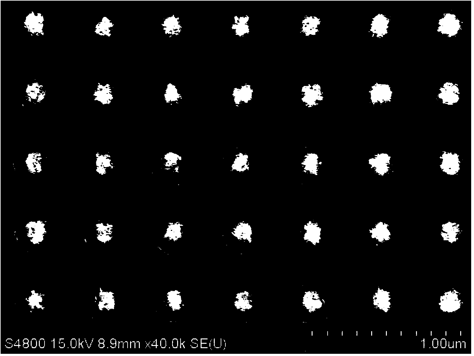
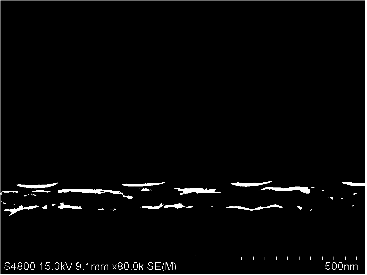
[0042] Using a Q...
PUM
| Property | Measurement | Unit |
|---|---|---|
| diameter | aaaaa | aaaaa |
| thickness | aaaaa | aaaaa |
| diameter | aaaaa | aaaaa |
Abstract
Description
Claims
Application Information