Backside-illuminated sensor

A sensor, back-illuminated technology, applied in the field of back-illuminated sensors, can solve the problems of reducing quantum efficiency, reducing sensor performance, etc., to achieve the effect of improving sensitivity and solving the problem of punch-through

Inactive Publication Date: 2009-04-01
TAIWAN SEMICON MFG CO LTD
View PDF0 Cites 10 Cited by
  • Summary
  • Abstract
  • Description
  • Claims
  • Application Information

AI Technical Summary

Problems solved by technology

However, thin substrates can also reduce sensor performance, such as reduced quantum efficiency (the ability to convert radiation into a signal), especially for visible light with long wavelengths (such as 650nm)

Method used


Image

  • Backside-illuminated sensor
  • Backside-illuminated sensor
  • Backside-illuminated sensor

Examples


Embodiment Construction

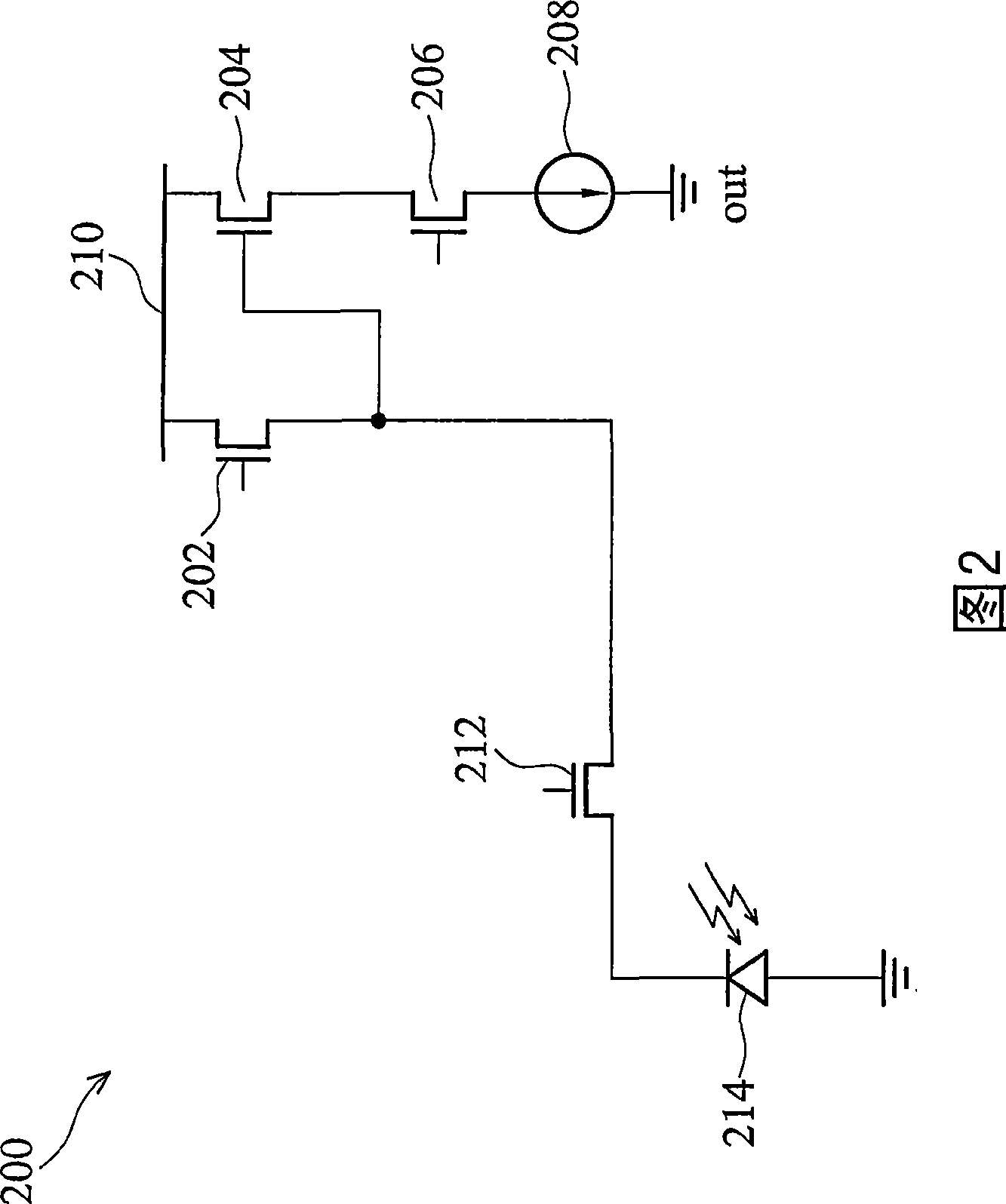
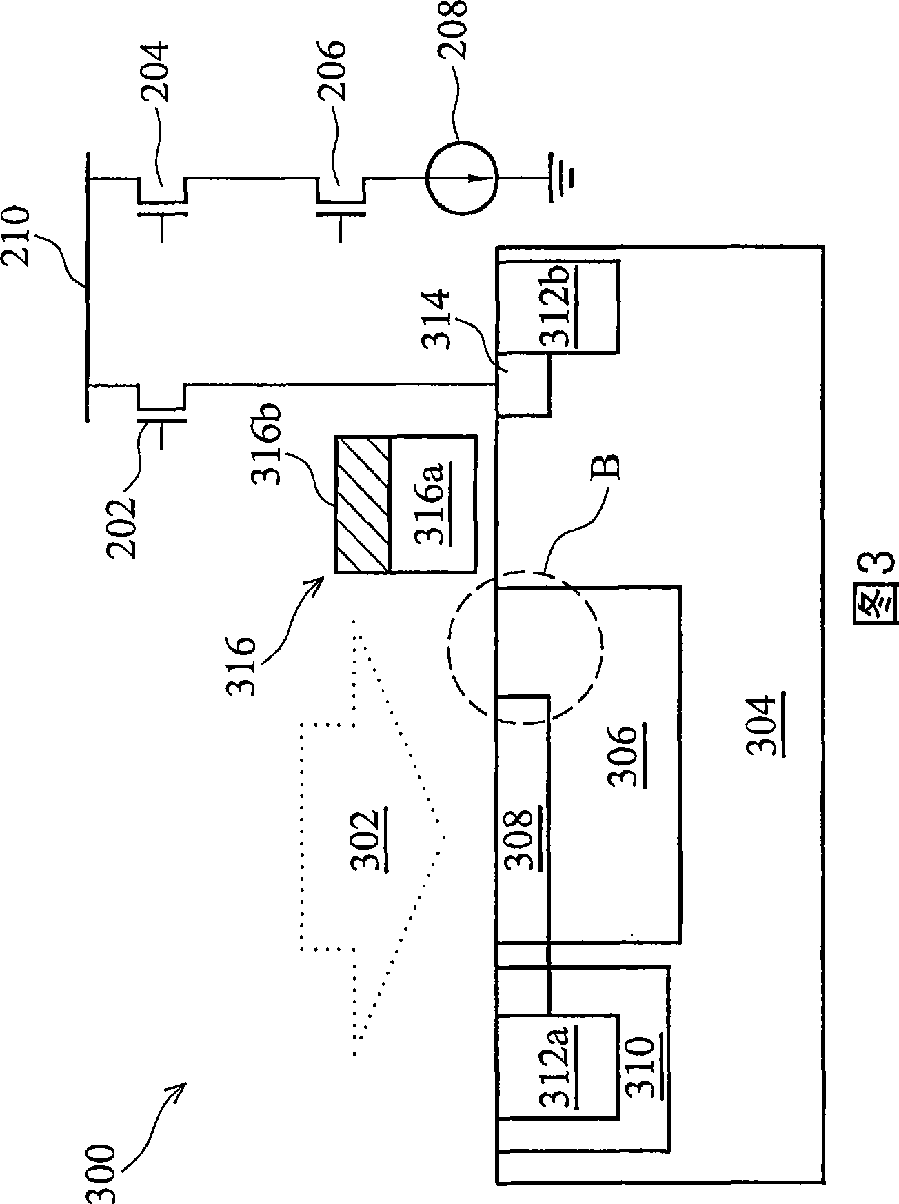
[0051] The present invention relates to an image sensor, and in particular to a back-illuminated image sensor. Although the present invention will be disclosed in several preferred embodiments, those of ordinary skill in the art can apply the methods disclosed in the present invention to other methods or devices. Moreover, the methods and devices disclosed in the present invention include some common structures and / or processes. Since these structures and processes are already known to those skilled in the art, they will only be discussed in general in this article. As for the repeated occurrence of reference signs in the reference figures, it is for the convenience of examples, and the repeated reference signs do not mean that they must be combined with the figures or steps in the figures. In addition, for the formation of the first characteristic pattern and the second characteristic pattern in the embodiments, if the following expressions are used, such as above, above, ov...


PUM


Abstract

Provides is a backside-illuminated sensor including a semiconductor substrate having a front surface and a back surface. A plurality of image sensor elements is formed on the front surface of the semiconductor substrate. At least one of the image sensor elements includes a transfer transistor and a photodetector. The gate of the transfer transistor includes an optically reflective layer. The gate of the transfer transistor, including the optically reflective layer, overlies the photodetector. In one embodiment, the gate overlies the photodetector by at least 5%. The invention can resolve the penetrating problem and improve the sensitivity for the image sensor element.

Description

technical field [0001] The present invention relates to a semiconductor device, and more particularly to a back-illuminated sensor. Background technique [0002] In the application of semiconductor technology, the back-illuminated sensor is used to sense the amount of radiation (such as light) projected on the back surface of the substrate. For this purpose, the image sensor uses an array of elements (such as pixels) to detect the amount of radiation. Each image sensing element includes at least one radiation sensing element, where the radiation sensing element refers to a light sensor. The light sensor can be located on the front side of the substrate, and the substrate must be thin enough to allow radiation incident on the backside of the substrate to reach the light sensor. Thin substrates reduce optical or electrical crosstalk between image sensor elements. However, thin substrates can also reduce sensor performance, such as reducing quantum efficiency (the ability to ...

Claims


Application Information

Patent Timeline
Patent Type & Authority Applications(China)
IPC IPC(8): H01L27/146
CPCH01L27/1464H01L27/14603H01L27/14625
Inventor 许慈轩杨敦年王俊智
Owner TAIWAN SEMICON MFG CO LTD
Why Eureka
Try Eureka