Electro-optical device and electronic apparatus

一种电光学装置、电极的技术,应用在电光源、辨认装置、照明装置等方向,能够解决发光亮度不均匀、有机EL薄膜困难、膜厚高度不均匀等问题

Inactive Publication Date: 2009-04-01
SEIKO EPSON CORP
View PDF1 Cites 26 Cited by
  • Summary
  • Abstract
  • Description
  • Claims
  • Application Information

AI Technical Summary

Problems solved by technology

Therefore, there is a problem that the droplet ejection region R surrounded by the partition walls 242 S When the droplet inside is dried and its surface is lowered, the droplet 245a will remain on the flat portion 251.
As a result, the film thickness of the organic EL thin film 245 after the droplets are dried becomes smaller than that in the droplet ejection region R. S The peripheral part becomes thinner and the film thickness is uneven
Moreover, there is also a problem that the film thickness of the organic EL thin film 245 becomes uneven around the portion where the first partition wall 243 and the organic EL thin film 245 are in contact.
[0007] In conventional electro-optic devices, in order to increase the area of ​​the light-emitting region, it is necessary to make the droplet discharge region a purely rectangular shape. However, in the rectangular droplet discharge region, an organic EL with a uniform height from the substrate surface is fabricated. Thin films are more difficult
As mentioned above, the non-uniformity of film thickness and surface height of these organic EL thin films becomes the cause of non-uniformity of luminance.

Method used


Image

  • Electro-optical device and electronic apparatus
  • Electro-optical device and electronic apparatus
  • Electro-optical device and electronic apparatus

Examples


no. 1 Embodiment approach

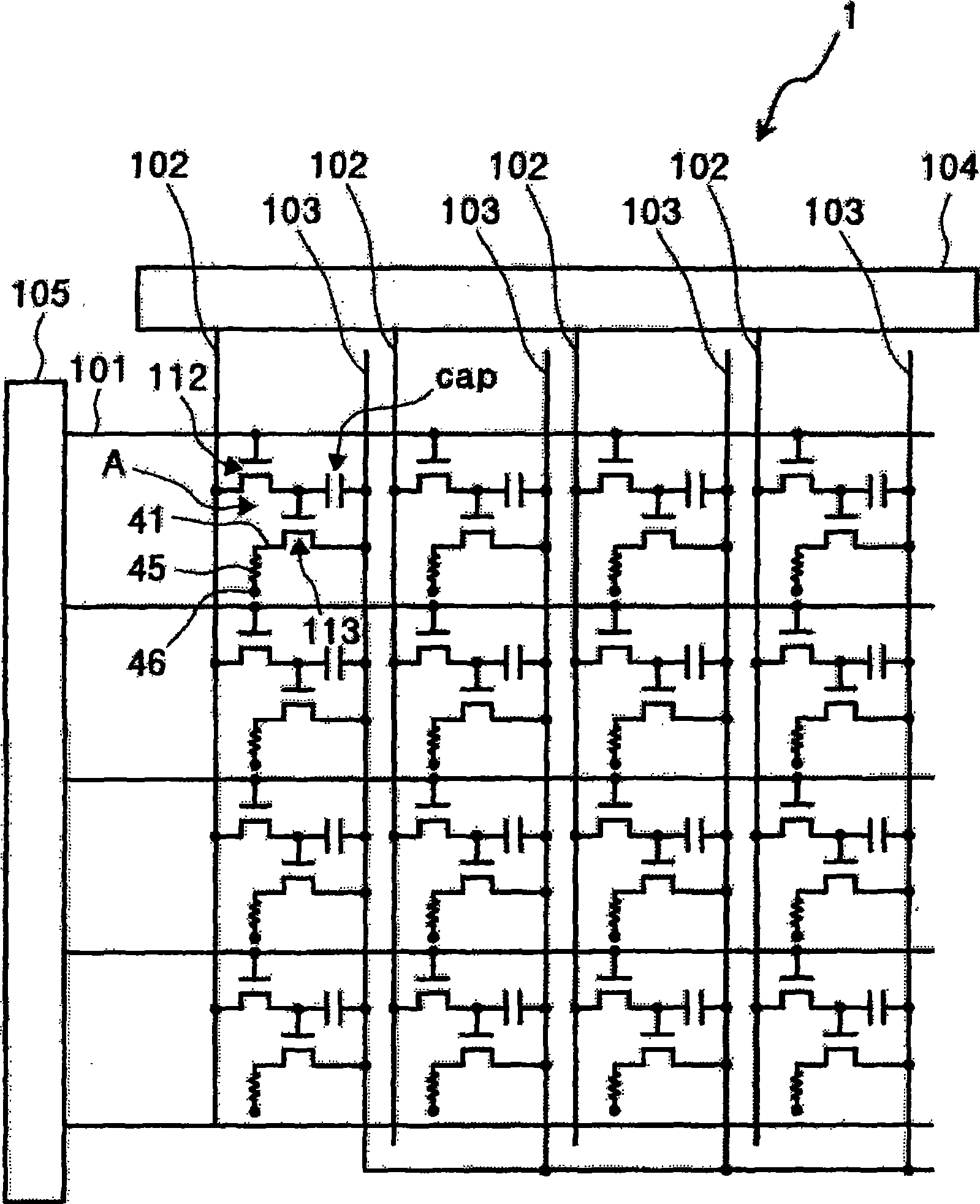
[0054] figure 1 A schematic plan view showing the wiring structure of the electro-optical device according to the present invention. as it should figure 1 As shown in , the electro-optical device 1 is respectively arranged with: a plurality of scanning lines 101; a plurality of signal lines 102 spaced apart from the scanning lines 101 and extending in a direction substantially perpendicular to each other; A plurality of power lines 103. Next, pixel regions A are provided in a matrix near each intersection of the scanning lines 101 and the signal lines 102 .

[0055] A data drive circuit 104 including a shift register, a level shifter, a video line, and an analog switch is connected to the signal line 102 . Furthermore, a scanning-side driver circuit 105 including a shift register and a level shifter is connected to the scanning line 101 .

[0056] The pixel area A is respectively provided with: a TFT 112 for switching, which supplies a scanning signal to the gate electro...

no. 2 Embodiment approach

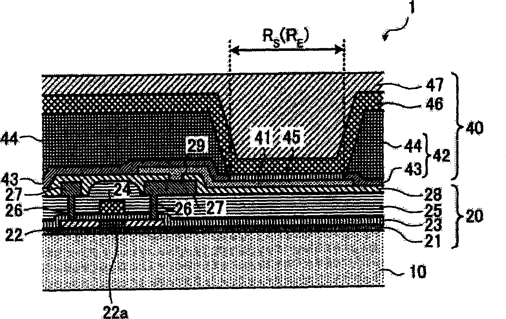
[0082] In the second embodiment, the configuration of the electro-optical device in the case where the functional layer 45 has at least a light-emitting layer and an auxiliary layer formed under the light-emitting layer will be described. Figure 9 A cross-sectional view showing a main part of a second embodiment of the electro-optical device according to the present invention. This electro-optical device is characterized in that the first partition wall 43a has a two-layer structure of the third partition wall 43aa and the fourth partition wall 43ab, and the partition wall 42a has a three-layer structure. The structure of the partition wall 42a includes: a third partition wall 43aa formed on the drive element portion 20, capable of surrounding the droplet ejection region R S and have lyophilicity; the fourth partition wall 43ab is formed on the third partition wall 43aa and has lyophilicity; the second partition wall 44a is formed on the fourth partition wall 43ab and has liq...

no. 3 Embodiment approach

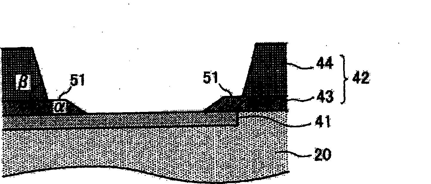
[0094] In this third embodiment, in the electro-optical device having a rectangular droplet ejection region, the region surrounding the first partition wall has a uniform film thickness, and the height of the surface of the functional layer in the droplet ejection region is The configuration of a uniform electro-optical device will be described.

[0095] Figure 10 A plan view showing the configuration of a third embodiment of the electro-optical device according to the present invention, Figure 11 express Figure 10 A—A sectional view of , and then Figure 12 express Figure 10 The B-B cross-sectional view. In these figures, only the droplet ejection region and the peripheral portion of the partition wall are shown. According to the electro-optical device of the third embodiment, the cross-sectional shape is the same as that of the second embodiment. Figure 9 Similarly, its partition wall 42a has a three-layer structure of the third and fourth partition walls 43aa, 43ab...


PUM

PropertyMeasurementUnit
cure temperatureaaaaaaaaaa

Abstract

This invention provides an electro-optical device having organic light emitting diode, comprising: a plurality of first electrodes mounted on a substrate; a partition having a first partition and a second partition; the first partition mounted at the circumference section of a plurality of first electrodes, consisting a side part and an upper part and having lyophily; the second partition formed on the upper part of the first partition and having lyophobicity; a functional layer mounted on the first electrode of the region surrounded by the first partition and the second partition, at least comprising an organic light emitting layer; a second electrode mounted on the function layer; a first opening section of the first partition is wider than a second opening section of the lower end of the second partition, thereby making a film thickness formed by drying liquid droplets filled in a liquid droplet ejection region surrounded by a partition be uniform.

Description

[0001] This application is a divisional application of the application number "200410092946.1", the filing date is November 11, 2004, and the invention title is "Electro-optical Device and Electronic Machine". technical field [0002] The present invention relates to an electro-optic device and a semiconductor device composed of an organic thin film. Furthermore, it also relates to an electronic device using an electro-optical device. Background technique [0003] In recent years, the development of electro-optical devices employing organic light emitting diodes (Organic Light Emitting Diodes (hereinafter referred to simply as "OLED elements" as appropriate) such as organic electroluminescent elements and light-emitting polymer elements as pixels has progressed. An OLED element has a structure in which an organic functional layer such as a light-emitting layer is interposed between an anode and a cathode. Recently, development of an electro-optical device employing a method...

Claims


Application Information

Patent Timeline
Patent Type & Authority Applications(China)
IPC IPC(8): H01L27/32H01L21/82H05B33/22B05D5/12B32B3/00G09F9/00G09F9/30H01L51/00H01L51/50H01L51/56H05B33/10H05B33/12H05B33/14
CPCH01L51/56H01L27/3246Y10T428/31504Y10T428/24917H10K59/122H10K71/40H05B33/22G09F9/30G09F9/00H05B33/10H10K71/00
Inventor 伊藤友幸野泽陵一
Owner SEIKO EPSON CORP
Why Eureka
Try Eureka