Solar cell

A technology of solar cells and hydrogenated amorphous silicon, which can be used in circuits, photovoltaic power generation, electrical components, etc., and can solve the problem of not being able to increase the size.

Inactive Publication Date: 2009-04-01
ARISE TECH CORP
View PDF8 Cites 63 Cited by
  • Summary
  • Abstract
  • Description
  • Claims
  • Application Information

AI Technical Summary

Problems solved by technology

The presence of electrical contacts on the front surface makes it problematic to apply an optimal anti-reflection layer on the front surface because the electrical contacts on the front surface need to be both transparent and conductive
Furthermore, since the contacts are located in the path of the incident light, the electrical contacts and busses on the front surface cannot be significantly oversized in order to further reduce the series resistance

Method used


Image

  • Solar cell
  • Solar cell
  • Solar cell

Examples


Embodiment Construction

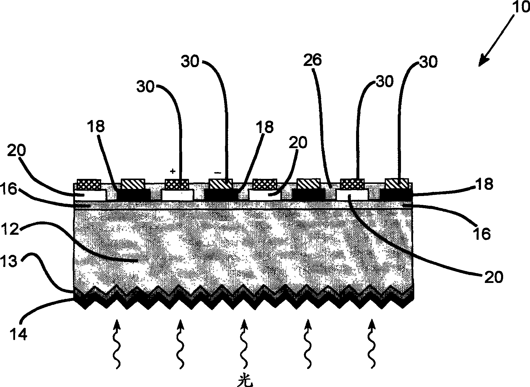
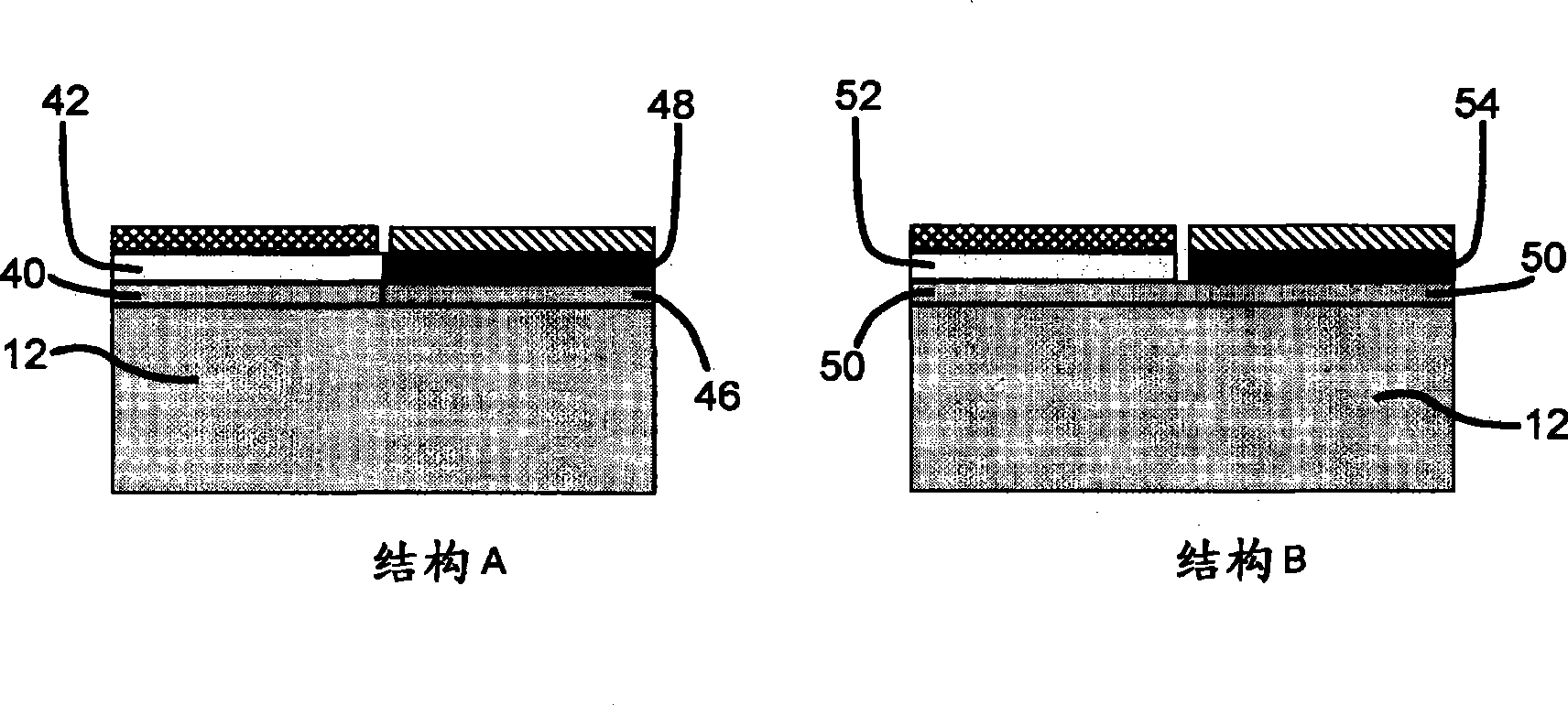
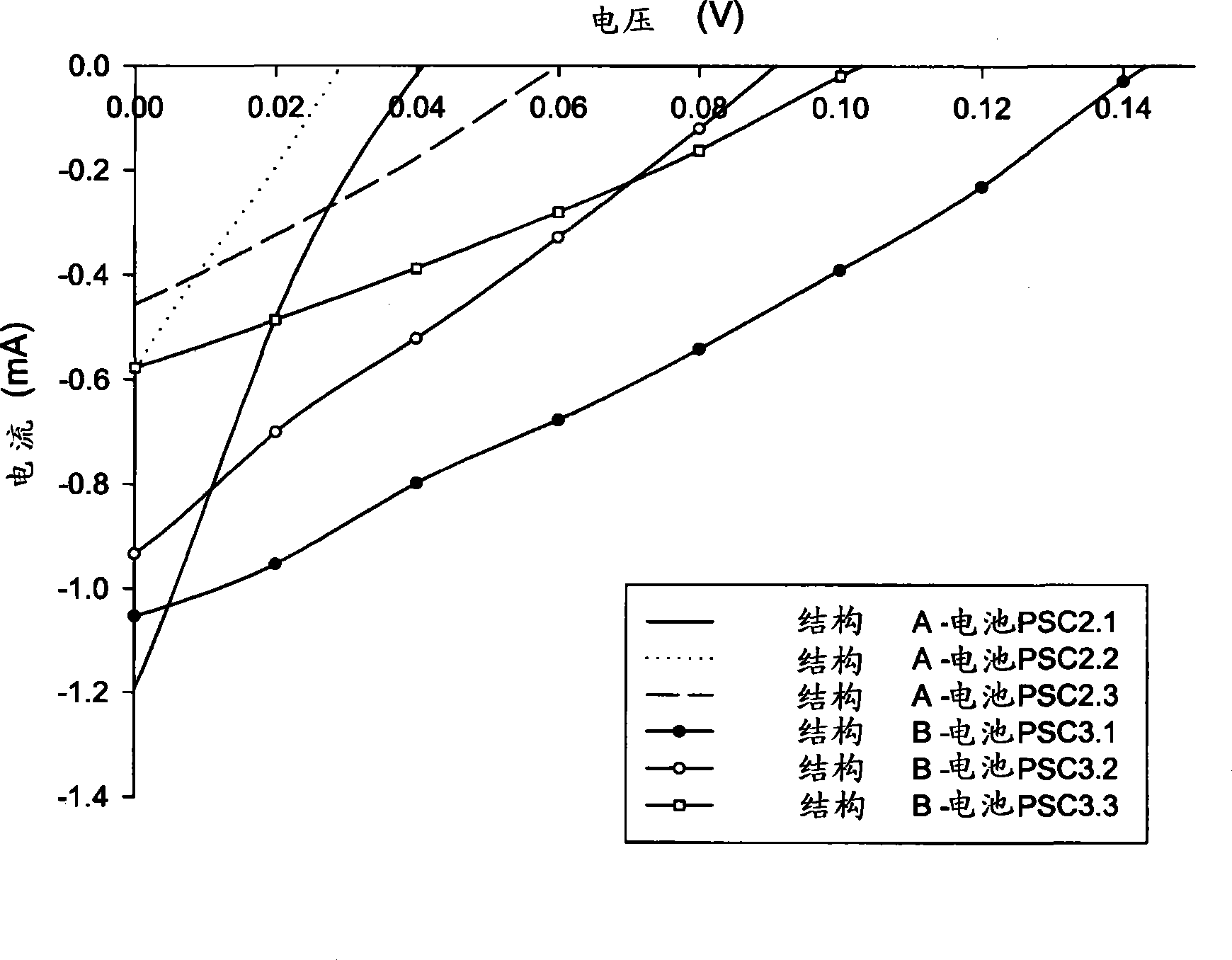
[0020] The systems described herein generally relate to solar cell implementations. Although embodiments of the invention are disclosed herein, the disclosed embodiments are exemplary only, and it should be understood that the invention is capable of many alternative forms. Furthermore, the figures are not to scale and some features may be exaggerated or minimized to show details of particular features, while related elements may be omitted to avoid obscuring novel aspects. Therefore, specific structural and functional details disclosed herein are not to be interpreted as limiting, but merely as a basis for the claims and as a representative basis for enabling one skilled in the art to variously employ the present invention. For purposes of instruction and not limitation, the illustrated embodiments relate to solar cell embodiments.

[0021] As used herein, the term "about" when referring to a range of dimensions such as layer thicknesses or other physical properties or chara...


PUM

PropertyMeasurementUnit
thicknessaaaaaaaaaa
thicknessaaaaaaaaaa

Abstract

The invention provides a thin film amorphous silicon-crystalline silicon back heterojunction and back surface field device configuration for a heterojunction solar cell. The configuration is attained by the formation of heterojunctions on the back surface of crystalline silicon at low temperatures. Low temperature fabrication allows for the application of low resolution lithography and / or shadow masking processes to produce the structures. The heterojunctions and interface passivation can be formed through a variety of material compositions and deposition processes, including appropriate surface restructing techniques. The configuration achieves separation of optimization requirements for light absorption and carrier generation at the front surface on which the light is incident, and in the bulk, and charge carrier collection at the back of the device. The shadowing losses are eliminated by positioning the electrical contacts at the back thereby removing them from the path of the incident light. Back contacts need optimization only for maximum charge carrier collection without bothering about shading losses. A range of elements / alloys may be used to effect band-bending.

Description

technical field [0001] The present invention relates to thin film back heterojunction, amorphous-crystalline silicon photovoltaic devices fabricated at low temperatures. Background technique [0002] Most of today's silicon optoelectronic devices are constructed by forming p-n junctions in silicon by diffusing dopants at high temperature and applying electrodes on the light and back sides. Back contacts formed on silicon photovoltaic devices are formed using high temperature processing to substantially overcome shading loss on the light-facing side. Amorphous-crystalline silicon heterojunction photovoltaic devices are formed by depositing an amorphous silicon layer on crystalline silicon, thus substantially providing low temperature processing. In this case, the electrodes are applied on the light-facing front side as well as on the rear side of the component. [0003] JP18413358 by Hamakawa et al. and US Patent No. 4,496,788 disclose amorphous (microcrystalline) / crystalli...

Claims


Application Information

Patent Timeline
Patent Type & Authority Applications(China)
IPC IPC(8): H01L31/0376H01L31/0216H01L31/0224
CPCH01L31/0745H01L31/022425H01L31/0747Y02E10/50H01L31/077H01L31/022441H01L31/02167Y02E10/547
Inventor 纳齐尔·皮亚拉利·凯拉尼巴努·甘加达尔·罗亚普罗尔达维特·叶吉克扬斯特凡·祖科廷斯基
Owner ARISE TECH CORP
Why Eureka
Try Eureka