
Eureka
For R&D, Eureka makes reading and utilizing patents & technical documents easy.
Eureka AIR
Designed for self-driven R&D workflows. Generate viable solutions, solve complex R&D challenges, empower your innovation with AI.

Eureka Materials
Designed for material experts only. Revolutionize your material R&D, from search, analyze, to developing new materials.

TechResearch
Generate reliable direction feasibility study reports for your R&D in just a few steps.

TechSeek
Discover and master advanced knowledge NOW. Basics, ideas, possibilities, all at once.

TechMind
As an expert in R&D Theories, TechMind can generates customized viable solutions instantly.

TechRisk
Analyze your overall solution with one click, know your potential R&D risks in advance.

TechMonitor
Get weekly tech updates, stay abreast of the latest tech innovations and key insights.
Optical element module and image pickup device
A technology of optical components and components, applied in the directions of optical components, optics, projection devices, etc., can solve the problem of no miniaturization, and achieve the effects of large deformation, small thickness and high elasticity
- Summary
- Abstract
- Description
- Claims
- Application Information
AI Technical Summary
Problems solved by technology
Method used
Image

Examples
Embodiment Construction
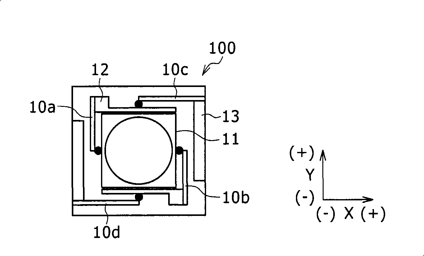
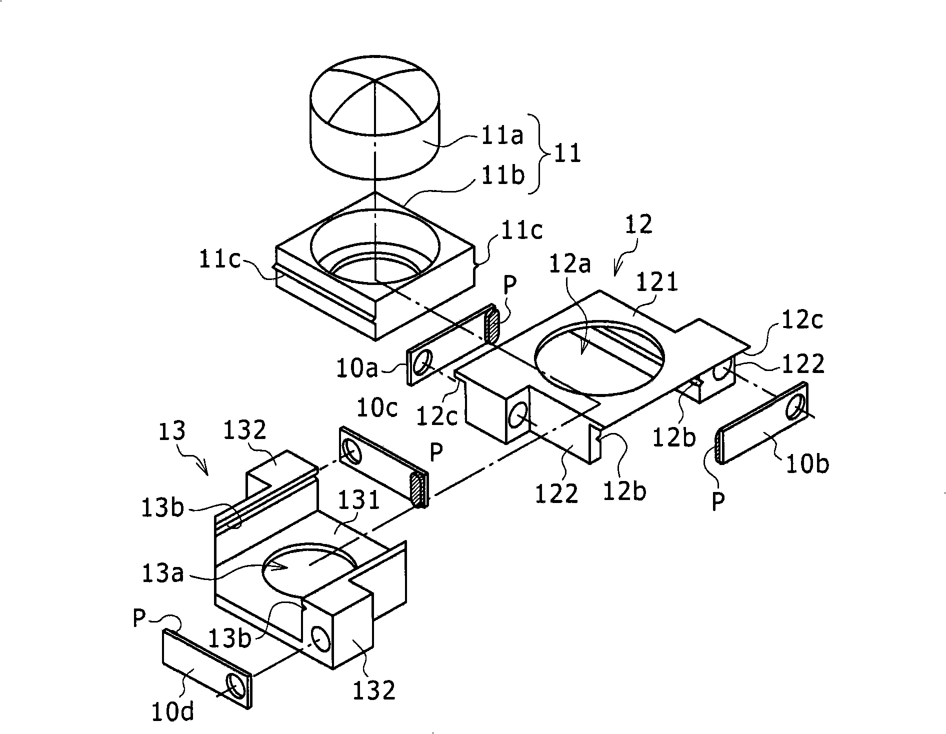
[0036]The structure of an optical element module according to an embodiment of the present invention will be described below. It should be noted that although the present invention will be described using the embodiments shown in the drawings, the present invention is not limited thereto. Appropriate changes can be made based on these embodiments. Any such embodiments are included in the scope of the present invention as long as the embodiments exert the actions and effects of the present invention.
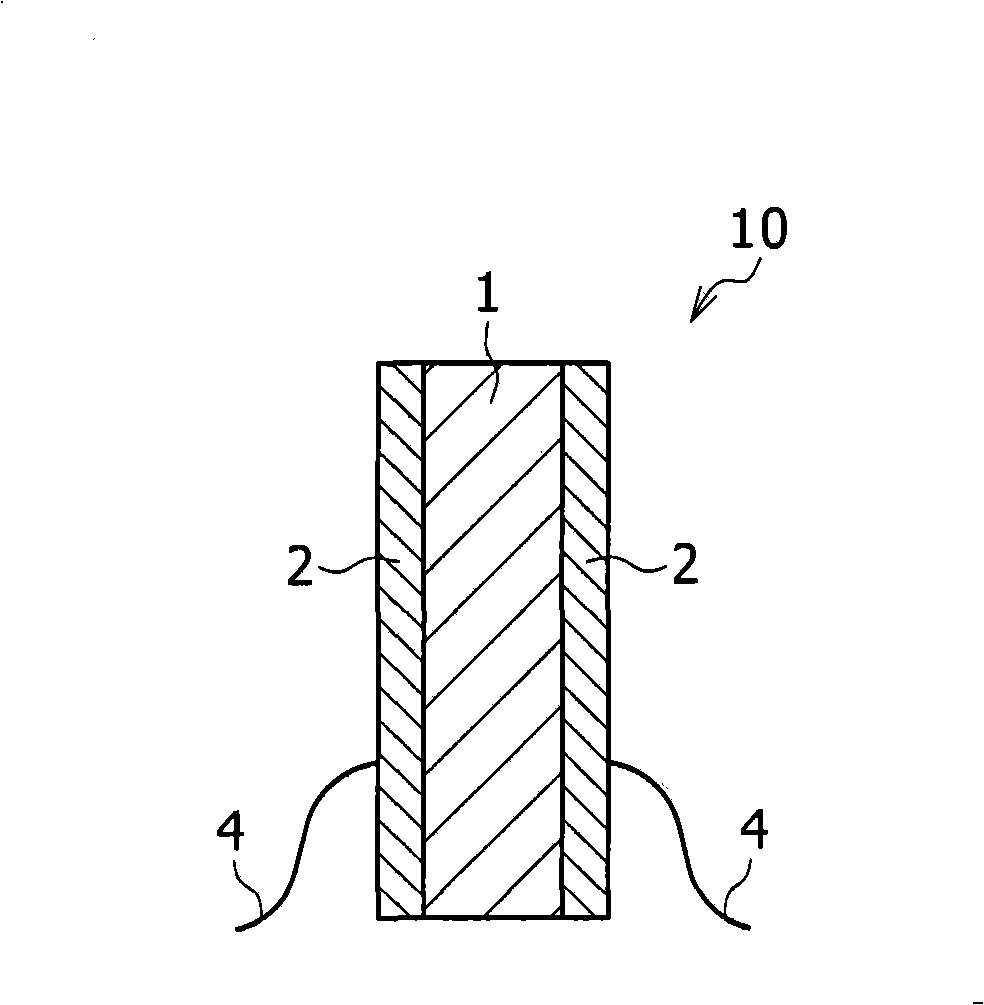
[0037] An optical element module according to an embodiment of the present invention includes: an optical element; and a plurality of actuator elements, each of which has a rectangular strip-shaped ion-conductive polymer film and an ion-conductive polymer film The electrodes on both sides of the electrode, the actuator element is bent as a whole in the thickness direction by applying a voltage between the electrodes; the optical element is moved on a plane perpendicular to the o...
PUM
 Abstract
Description
Claims
Application Information
 - R&D Engineer
- R&D Manager
- IP Professional
- Industry Leading Data Capabilities
- Powerful AI technology
- Patent DNA Extraction
Browse by: Latest US Patents, China's latest patents, Technical Efficacy Thesaurus, Application Domain, Technology Topic, Popular Technical Reports.
© 2024 PatSnap. All rights reserved.Legal|Privacy policy|Modern Slavery Act Transparency Statement|Sitemap|About US| Contact US: help@patsnap.com