Solid state imaging device, its manufacturing method, and imaging device

A solid-state imaging device and technology for imaging devices, which are applied in semiconductor/solid-state device manufacturing, radiation control devices, image communication, etc., can solve problems such as difficulty in implementing an insulating layer, and achieve the effect of noise reduction

Active Publication Date: 2009-04-15
SONY CORP
View PDF2 Cites 23 Cited by
  • Summary
  • Abstract
  • Description
  • Claims
  • Application Information

AI Technical Summary

Problems solved by technology

For this reason, it is difficult to realize the insulating layer because a high-

Method used


Image

  • Solid state imaging device, its manufacturing method, and imaging device
  • Solid state imaging device, its manufacturing method, and imaging device
  • Solid state imaging device, its manufacturing method, and imaging device

Examples


Embodiment Construction

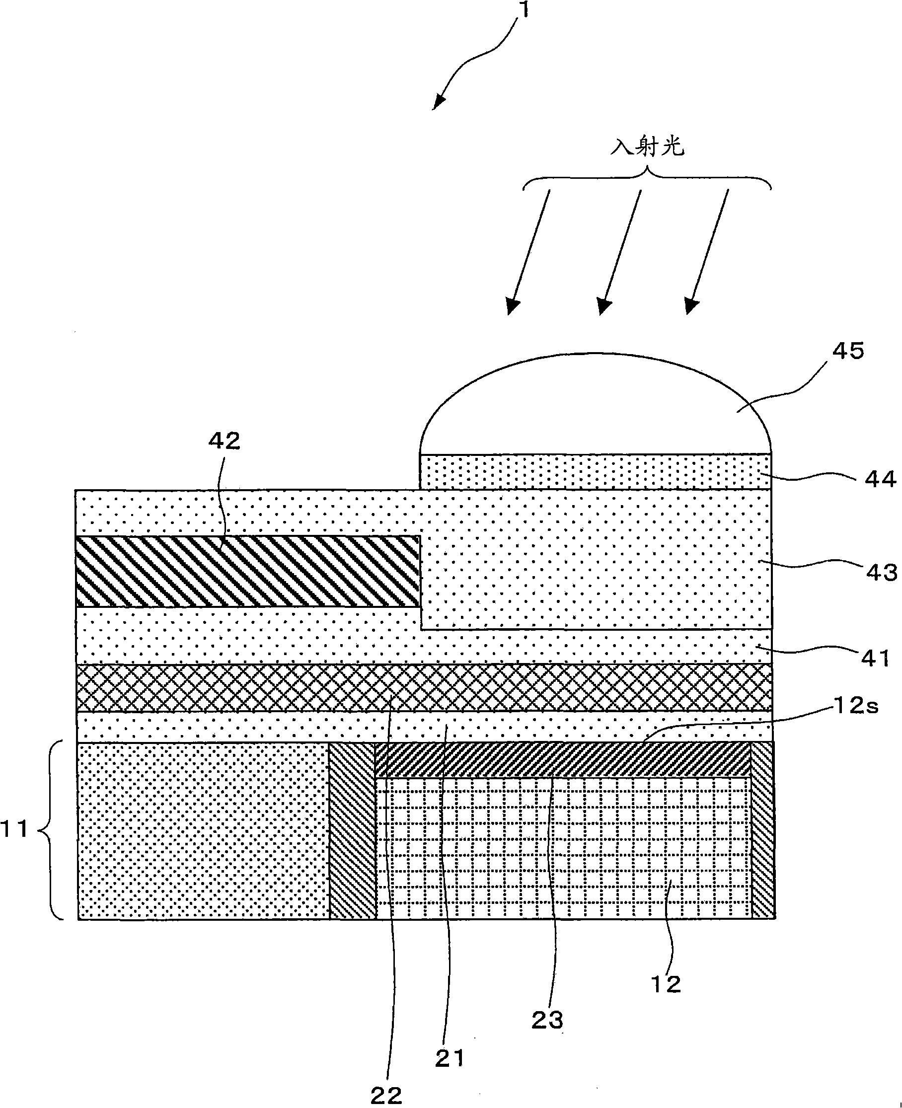
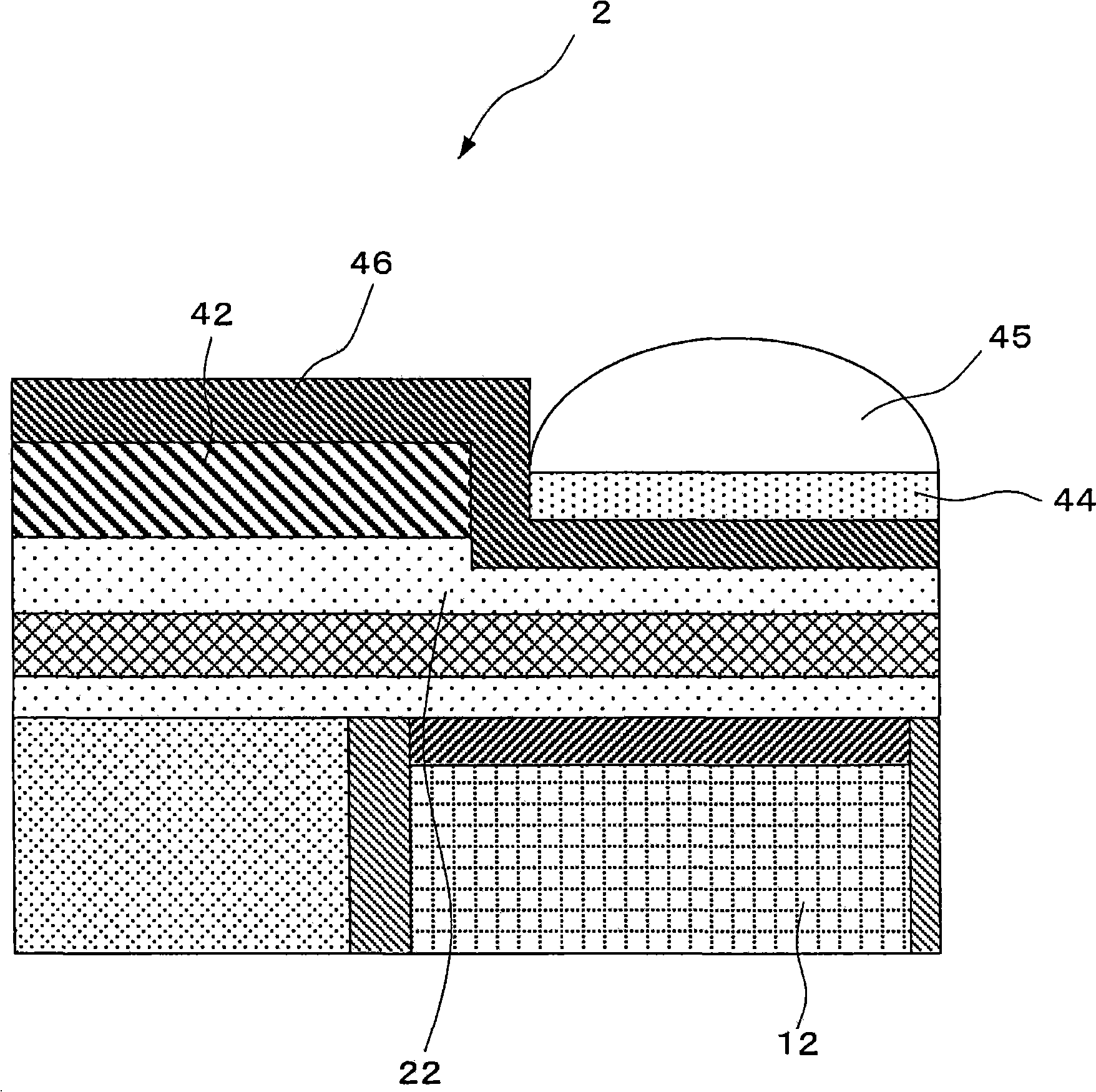
[0076] The following will refer to the figure 1 A cross-sectional view of a solid-state imaging device (first solid-state imaging device) according to an embodiment (first example) of the present invention will be described.

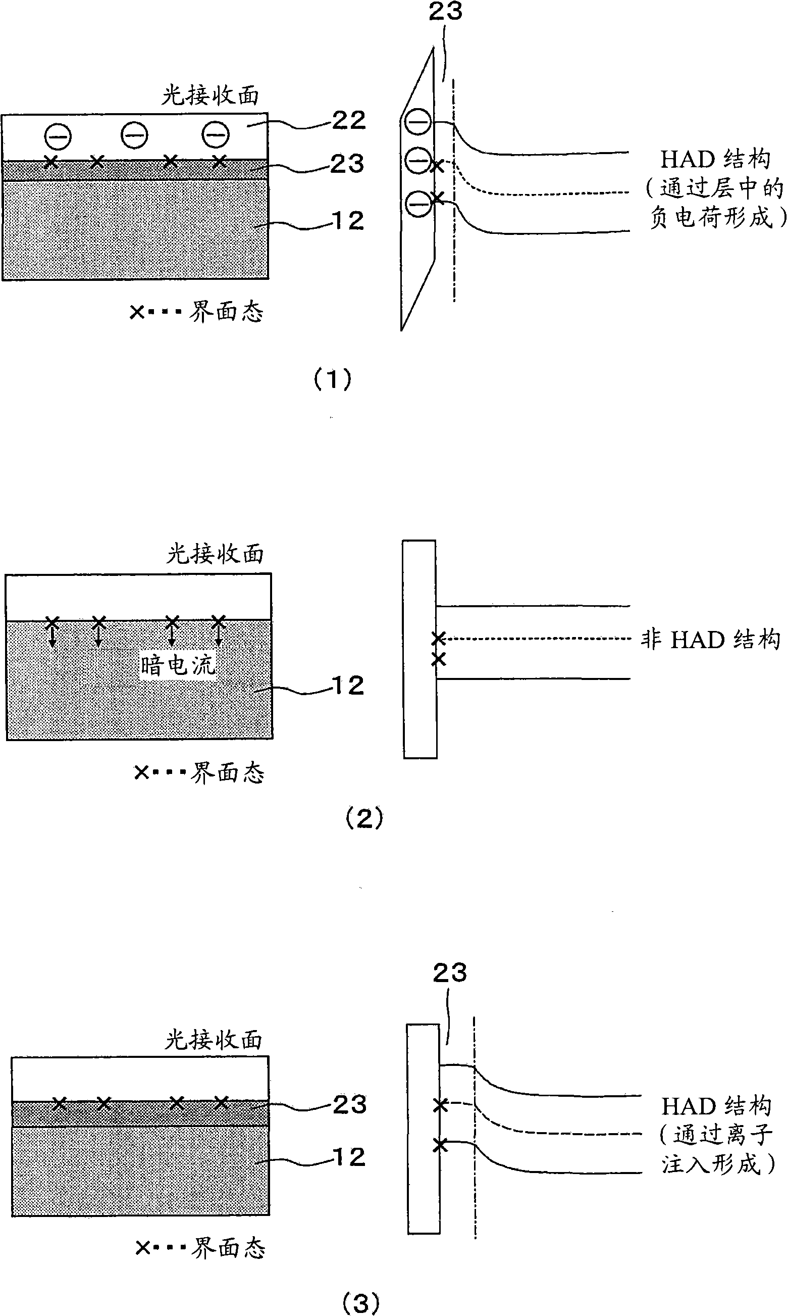
[0077] Such as figure 1 As shown, the solid-state imaging device 1 includes a photosensitive portion 12 that performs photoelectric conversion of incident light L in a semiconductor substrate (or semiconductor layer) 11 . On the side portion of the photosensitive portion 12 , a peripheral circuit portion 14 formed with a peripheral circuit (not specifically shown) is provided with the pixel separation region 13 interposed therebetween. The following description will be made using the semiconductor substrate 11 . On the light-receiving face 12s of the photosensitive portion (including a hole collection layer 23 to be described later) 12, an interface state lowering layer 21 is formed. The interface state reduction layer 21 is made of, for example, si...


PUM


Abstract

The invention discloses a solid state imaging device having a light sensing section that performs photoelectric conversion of incident light and an imaging device, including: an insulating layer formed on a light receiving surface of the light sensing section; a layer having negative electric charges formed on the insulating layer; and a hole accumulation layer formed on the light receiving surface of the light sensing section. According to the solid image device of the invention, dark current is reduced, noises in the images are reduced, as a result, the invention has the advantages of high image.

Description

[0001] Cross References to Related Applications [0002] The present invention contains subject matter of Japanese Patent Application No. 2007-265287 filed in the Japan Patent Office on October 11, 2007, the entire content of which is hereby incorporated by reference. technical field [0003] The present invention relates to a solid-state imaging device capable of suppressing dark current generation, a manufacturing method thereof, and an imaging device. Background technique [0004] Solid-state imaging devices such as CCDs (Charge Coupled Devices) and CMOS image sensors are widely used in video cameras, digital cameras, and the like. In all types of solid-state imaging devices, sensitivity improvement and noise reduction are important issues. [0005] In particular, in a state where there is no incident light, even if there is no pure signal charge generated by photoelectric conversion of incident light, when charges (electrons) generated due to minute defects in the subst...

Claims


Application Information

Patent Timeline
IPC IPC(8): H01L27/146H01L21/822H04N5/225
CPCH01L27/14621H01L27/14627H01L27/14692
Inventor 押山到安藤崇志桧山晋山口哲司大岸裕子池田晴美
Owner SONY CORP
Why Eureka
Try Eureka