Methods for low cost manufacturing of complex layered materials and devices

A device and manufacturing process technology, applied in the field of composite layered materials and device manufacturing, can solve problems such as restricting the applicability of reel-to-reel production methods, restricting product design, and having no outer surface, so as to reduce R&D execution costs and improve productivity. , the effect of reducing waste

Inactive Publication Date: 2009-04-15
迈克罗拉布诊断有限公司
View PDF15 Cites 8 Cited by
  • Summary
  • Abstract
  • Description
  • Claims
  • Application Information

AI Technical Summary

Problems solved by technology

This limits the layer thicknesses employed and the number of layers that can be combined and manipulated on this line
This is problematic for many layered material applications that require larger environmental interfaces, larger fluid capacities, larger operational structures, or higher part strength, or a large number of bonded layers, all of which feature both tend to make the resulting devices rather rigid and thus severely limit the applicability of reel-to-reel production methods
[0025] Another disadvantage of reel-to-reel handling systems is that the substrate needs to maintain a generally planar shape with little or no protrusions on the outer surface
Because this method also defines the substrate thickness, which further limits the design of the product, often requiring larger 3-dimensional shaped objects to provide functionality such as connection to external devices or provision of internal liquid storage chambers

Method used


Image

  • Methods for low cost manufacturing of complex layered materials and devices
  • Methods for low cost manufacturing of complex layered materials and devices
  • Methods for low cost manufacturing of complex layered materials and devices

Examples


Embodiment Construction

[0131] The invention is described herein with respect to the disclosed embodiments in relation to microfluidic devices. However, the invention is applicable to a wide variety of situations and products, and it should be appreciated that other configurations and arrangements are considered to be within the scope of the invention. Various modifications, alterations, changes and / or additions to the constructions and arrangements described herein are also considered to fall within the metes and bounds of the present invention.

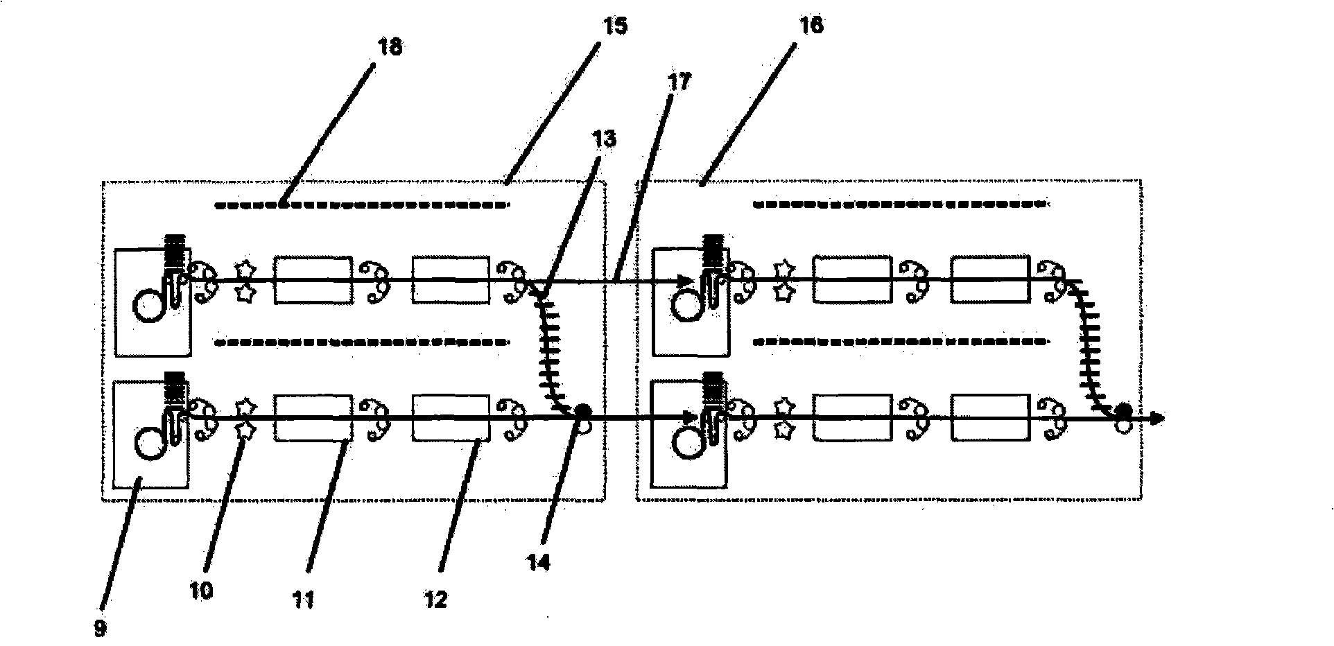
[0132] By combining reel-to-reel processing techniques and sheet handling systems into a flexible manufacturing strategy that can fabricate planar and non-planar devices of arbitrary thickness and with precise 3-dimensional surface and internal features, the manufacturing method of the present invention overcomes the aforementioned batch, serial and Limitations of reel-to-reel fabrication of layered materials and devices. Other novel manufacturing methods...


PUM


Abstract

A process for manufacturing a device includes performing a plurality of non-bonding processes during at least one web-based manufacturing stage and during at least one sheet-based manufacturing stage. The processes may be performed by a plurality of modules. The modules may be independently controlled and / or monitored. The modules may be interchangeable. One or more modules may receive and / or pass material to another module. The devices that are manufactured may be a layered device, a smart card, a sensor, an actuator, an in vitro diagnostic device, a microfluidic device, or a laminar product. An apparatus for manufacturing device includes at least one web-based manufacturing component and at least one sheet-based manufacturing component. The at least one web-based manufacturing component and the at least one sheet-based manufacturing component are configured to perform a plurality of non-bonding processes.

Description

technical field [0001] The present invention generally relates to the fabrication of composite layered materials and devices having one or more layers of suitably modified, altered or added materials. More particularly, the present invention relates to methods of manufacturing these materials and devices at low cost, in variable quantities, and at the same time with a high degree of variability and precision complexity, under varying degrees of manual or automatic control. Additionally, the present invention relates to methods for efficiently fabricating layered materials and devices of varying functionality and complexity using the same fabrication facility. The field of the invention also extends to the efficient fabrication of complex polymeric materials and devices, the fabrication of which features variable and controllable dimensions from centimeters to nanometers. Background technique [0002] In the following discussion, reference is made to specific structures and / ...

Claims


Application Information

Patent Timeline
Patent Type & Authority Applications(China)
IPC IPC(8): B32B37/22B32B37/02
Inventor 迈卡·J·阿特金格雷戈里·F·伊顿
Owner 迈克罗拉布诊断有限公司
Why Eureka
Try Eureka