Mini camera module and method for producing the same

The technology of a camera module and its manufacturing method, which is applied in the field of optical imaging, can solve the problems that the camera module is large in size and difficult to integrate

Inactive Publication Date: 2009-04-29
HONG FU JIN PRECISION IND (SHENZHEN) CO LTD +1
View PDF0 Cites 5 Cited by
  • Summary
  • Abstract
  • Description
  • Claims
  • Application Information

AI Technical Summary

Problems solved by technology

However, as mobile phones are becoming more and more thinner and smaller, traditional camera modules are difficult to integrate into mobile phones due to their large size so that mobile phones can also have camera functions.

Method used


Image

  • Mini camera module and method for producing the same
  • Mini camera module and method for producing the same
  • Mini camera module and method for producing the same

Examples


no. 1 example

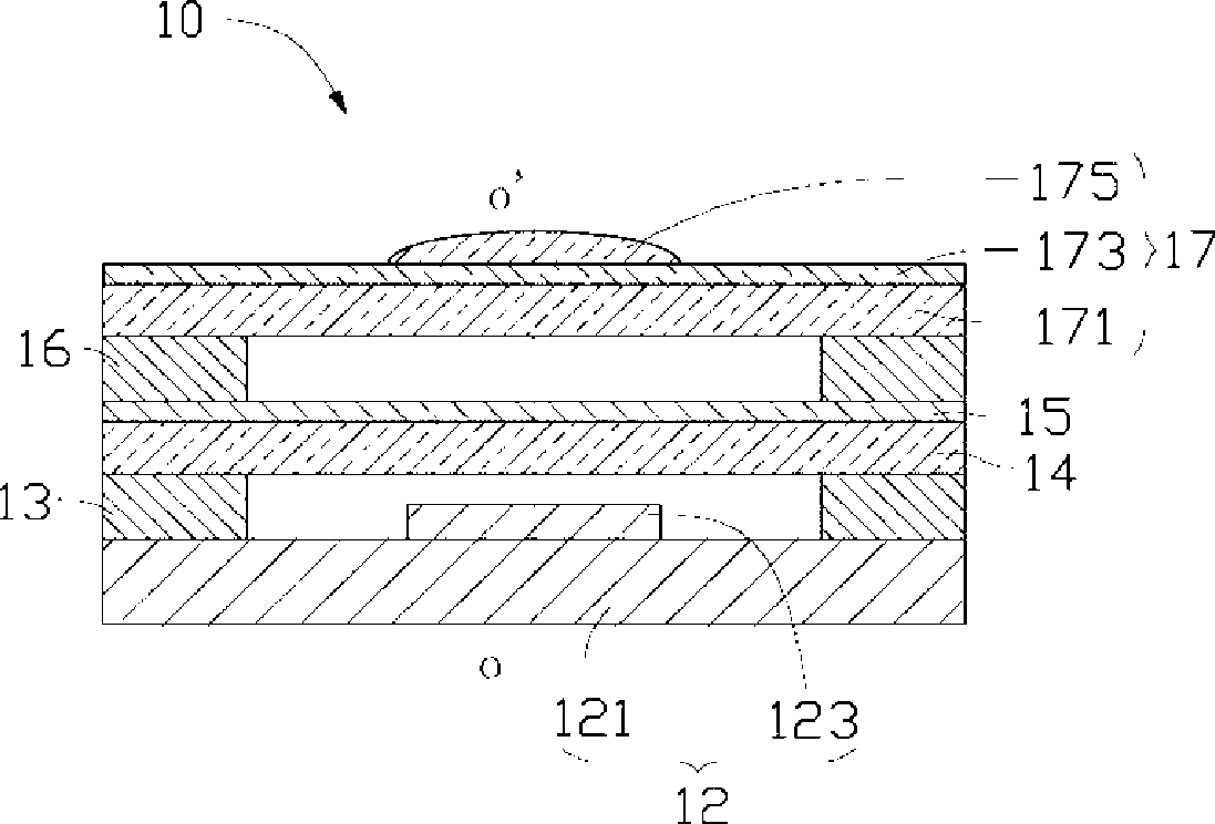
[0022] see figure 1 , the miniature camera module 10 provided by the first embodiment of the present invention includes an image sensing unit 12, a spacer layer 13, a transparent cover plate 14, an infrared cut filter (Infra-red Cut Filter) layer 15, A spacer unit 16 and a lens unit 17 .

[0023] The image sensing unit 12 is a solid-state image sensing device, such as a charge-coupled sensing device (CCD) or a complementary metal-oxide-semiconductor device (CMOS). The image sensing unit may include a semiconductor substrate 121 and a photosensitive region 123 formed on one side of the semiconductor substrate 121 through a semiconductor process; the semiconductor substrate 121 may be a silicon substrate.

[0024] The spacer layer 13 is bonded to one side of the image sensing unit 12 where the photosensitive region 123 is formed, and is a ring structure, such as a square ring structure. The square ring structure may have a square outline and a circular through hole. The space...

no. 2 example

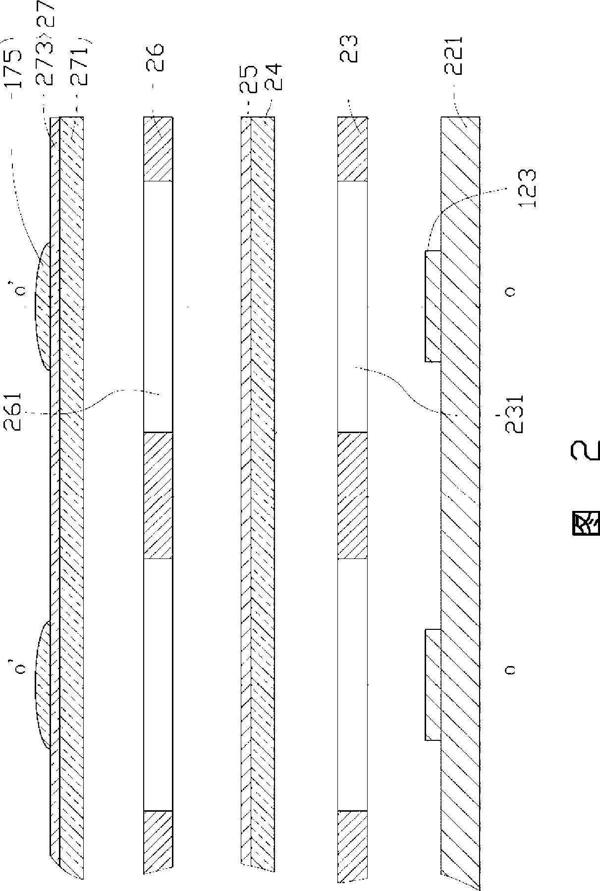
[0041] see Figure 4 The micro camera module 30 provided by the second embodiment of the present invention is basically the same as the micro camera module 10 provided by the first embodiment, including an image sensing unit 12, a spacer layer 13, a transparent cover plate 14, An infrared cut filter (Infra-red Cut Filter) layer 15, a spacer unit 16 and a lens unit 17; the image sensing unit 12 includes a semiconductor substrate 121 and a semiconductor substrate 121 formed on one side The photosensitive area 123. The difference is that the miniature camera module 30 further includes a lens unit 37 and another spacer unit 16 between the lens unit 37 and the lens unit 17 . The lens unit 37 includes a glass substrate 371 , a transparent nucleation layer 373 on the glass substrate 371 , and a lens 375 on the transparent nucleation layer 373 . The lens 375 of the lens unit 37 is arranged on the main optical axis OO′ of the lens 175 of the lens unit 17, and the lens unit 37 is bond...


PUM


Abstract

The invention relates to a miniature camera module and a manufacturing method thereof. The miniature camera module comprises an image sensing unit and a lens unit, wherein the image sensing unit comprises a photosensitive region; the lens unit is connected to the image sensing unit close to the photosensitive region side; the lens unit comprises a glass substrate, a transparent nucleating layer positioned on the glass substrate and a lens positioned on the transparent nucleating layer; the lens is provided with a primary optical axis; and the photosensitive region is arranged on the primary optical axis of the lens and arranged at intervals with the lens unit. The miniature camera module controls the surface tension in the forming process of the lens and increases adhesive force between the lens and the glass substrate through controlling the lens unit by the arranged transparent nucleating layer. On the one hand, over shrinkage of the lens in the forming process of the lens caused by overlarge surface tension can be inhibited; one the other hand, the lens and the glass substrate can be closely combined so as not to fall off.

Description

technical field [0001] The invention relates to the field of optical imaging, in particular to a miniature camera module and a manufacturing method thereof. Background technique [0002] In recent years, electronic products with a camera function, such as mobile phones (Mobile Phone), are increasingly favored by consumers. However, as mobile phones are becoming thinner and smaller, it is difficult for traditional camera modules to be integrated into mobile phones so that the mobile phone can also have a camera function due to their large size. [0003] See the article "Novel Wafer Level Package Technology Studies for ImageSensor Devices" published by Gautham Viswanadam et al. at the 2005 Electronics Packaging Technology Conference, which discloses a micro-camera module that adopts wafer-level packaging, including a semiconductor image sensing chip ( Semiconductor Imaging Chip) and a lens module assembled with a semiconductor image sensor chip to form a single module (Single...

Claims


Application Information

Patent Timeline
Patent Type & Authority Applications(China)
IPC IPC(8): G02B7/02H01L27/146H01L21/50H04N5/225
CPCH01L27/14625H01L27/14618H01L2924/0002H01L2924/00
Inventor 陈杰良李俊佑
Owner HONG FU JIN PRECISION IND (SHENZHEN) CO LTD
Why Eureka
Try Eureka