

LCD and making method thereof
A liquid crystal display device and common electrode technology, applied in semiconductor/solid-state device manufacturing, optics, instruments, etc., can solve problems such as reducing the aperture ratio of display units, and achieve the effects of weakening undesirable phenomena, enhancing charge retention, and improving flickering
- Summary
- Abstract
- Description
- Claims
- Application Information
AI Technical Summary
Problems solved by technology
Method used
Image

Examples
Embodiment Construction
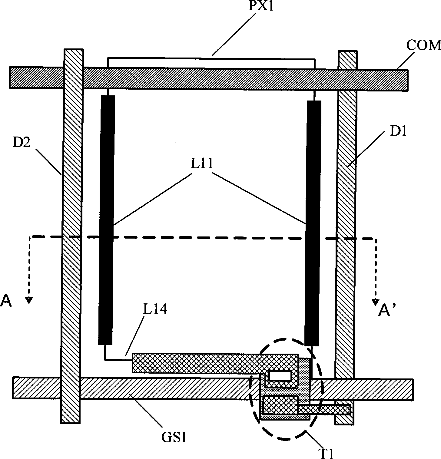
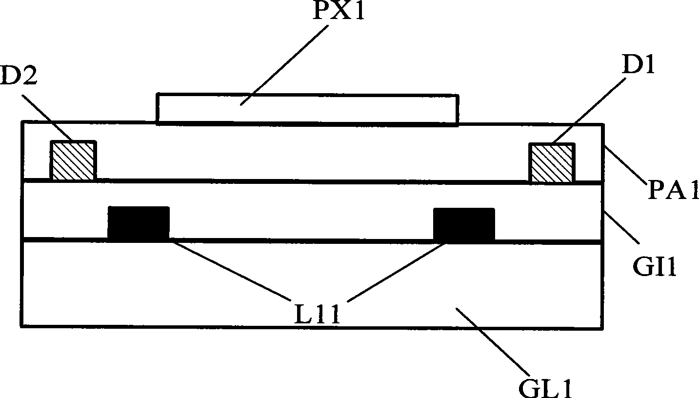
[0032] The liquid crystal display device and its manufacturing method of the present invention will be further described in detail below with reference to the accompanying drawings.
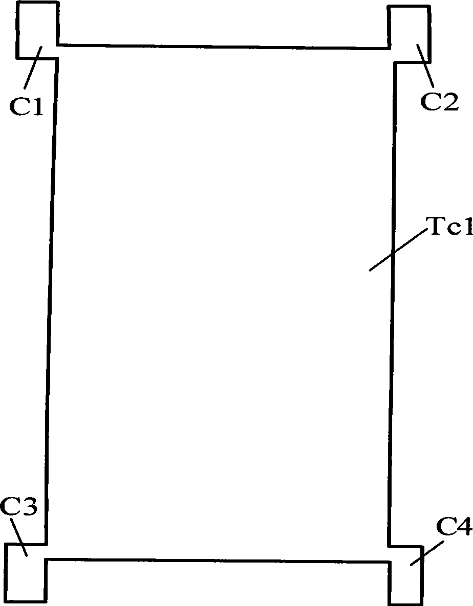
[0033] Such as Figure 7 As shown, the liquid crystal display device of the present invention has an array substrate, each display unit of the array substrate includes two data lines D3, D4 arranged in parallel, and the gate scan line GS2 straddles the data lines D3, D4 and the data lines D3, D4 Arranged crosswise, the data lines D3, D4 and the gate scanning line GS2 form a pixel area, and there is a pixel electrode PX2 in the pixel area, and the light-shielding strips L12 on both sides of the pixel electrode PX2 are used to prevent light leakage. The pixel electrode PX2 passes through the transistor T2 Connected to the data line D3 and the gate scanning line GS2, the transparent common electrode Tc1 located under the pixel electrode PX1, the transparent common electrode Tc1 is connected to the p...
PUM
 Abstract
Description
Claims
Application Information