Preparation method of back contact HIT solar battery based on N-type silicon wafer

A solar cell, back-contact technology, applied in circuits, electrical components, final product manufacturing, etc., can solve the problems of high cost and small production capacity, achieve the effect of simple method, reduce component production cost, and avoid electrode shading

Active Publication Date: 2013-08-21
山东力诺太阳能电力股份有限公司
View PDF6 Cites 2 Cited by
  • Summary
  • Abstract
  • Description
  • Claims
  • Application Information

AI Technical Summary

Problems solved by technology

However, most of them use laser technology, which has high cost and low production capacity.
The HIT battery reduces the thickness of the battery and improves the efficiency compared with the conventional crystalline silicon battery, but it still prints silver electrodes on the front of the battery, and the problem of shading rate has not been solved.

Method used


Image

  • Preparation method of back contact HIT solar battery based on N-type silicon wafer
  • Preparation method of back contact HIT solar battery based on N-type silicon wafer
  • Preparation method of back contact HIT solar battery based on N-type silicon wafer

Examples


Embodiment 1

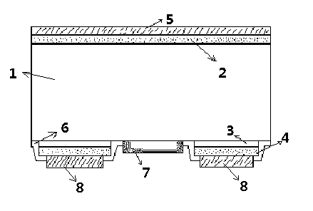
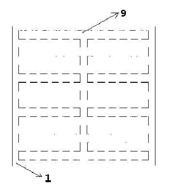
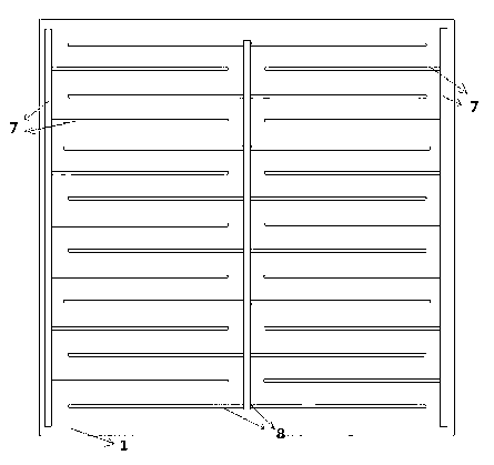
[0031] Select N-type monocrystalline silicon wafer; N-type silicon wafer 1 undergoes a conventional cleaning process, and the surface of the N-type silicon wafer is subjected to alkali texturing, so as to remove the mechanical damage layer on the surface of the silicon wafer, remove surface oil and metal impurities, and form a pyramid-like texture. Increase the absorption of sunlight, increase the area of ​​the PN junction, and increase the short-circuit current. Use amorphous silicon coating equipment to deposit a layer of highly doped N+ type amorphous silicon thin layer 2 on the front surface of N-type silicon wafer 1, with a film thickness of 50nm, and then deposit a layer on the back surface of N-type silicon wafer 1 in sequence An intrinsic amorphous silicon thin layer 3 with a film thickness of 1 nm, and a P-type amorphous silicon thin layer 4 with a film thickness of 150 nm. On the screen printing machine, according to the attached drawings figure 2 The mask pattern ...

Embodiment 2

[0033] Choose N-type polysilicon wafers; N-type silicon wafers 1 undergo conventional cleaning processes, and the surface is acid-textured in order to remove the mechanical damage layer on the surface of the silicon wafer, remove surface oil and metal impurities, and form an undulating suede surface to increase sunlight resistance. The absorption increases the PN junction area and increases the short-circuit current. Use amorphous silicon coating equipment to deposit a layer of highly doped N+ type amorphous silicon thin layer 2 on the upper surface of N-type silicon wafer 1, the film thickness is 50nm, and then deposit a layer on the back surface of N-type silicon wafer 1 in sequence An intrinsic amorphous silicon thin layer 3 with a film thickness of 1 nm, and a p-type amorphous silicon thin layer 4 with a film thickness of 150 nm. On the screen printing machine, according to the attached drawings figure 2 The mask pattern shown in , on the back surface of the N-type silic...


PUM


Abstract

The invention discloses a preparation method of a back contact HIT solar battery based on an N-type silicon substrate. The preparation method combines a conventional crystalline silicon battery productive technology and a thin film solar cell productive technology, is simple and is capable of realizing industrialization fast. The solar battery prepared by the method does not have the light-induced degradation phenomenon of the crystalline silicon solar battery; the transmission optical path of the sunlight in the battery is longer, and the thickness of the battery is greatly reduced than thatof the conventional crystalline silicon solar cell; the electrodes are fully printed on the back of the battery, thus not only avoiding the shading problem of the positive electrode of the conventional solar battery, but also reducing the requirements on the printing precision and height to width ratio of the electrode; in the component production process, by using the solar battery, welding processes can be reduced, solder strips are reduced and production cost of the component is lowered.

Description

technical field [0001] The invention relates to a method for preparing a solar cell, in particular to a method for preparing a back-contact HIT solar cell on an N-type silicon substrate. Background technique [0002] The rapid development of the solar energy industry requires an industrialized technology with simple process flow and high photoelectric conversion efficiency to reduce the cost of power generation and achieve the goal of being equal to or lower than the price of mains electricity. [0003] With the development of industrialization, conventional crystalline silicon cells have made great progress in improving conversion efficiency and reducing costs. However, the technical characteristics of conventional crystalline silicon cells limit the further reduction of their power generation costs, and it is difficult to achieve the goal of the same price as the mains electricity. Various solutions have emerged in the industry, including selective emitter solar cells, ba...

Claims


Application Information

Patent Timeline
Patent Type & Authority Patents(China)
IPC IPC(8): H01L31/18H01L31/20
CPCY02P70/50
Inventor 杨青天徐振华刘鹏姜言森李玉花程亮王兆光张春艳任现坤
Owner 山东力诺太阳能电力股份有限公司
Why Eureka
Try Eureka