Method of preparing solar cell on N-type silicon substrate
A technology for solar cells and silicon substrates, applied in circuits, photovoltaic power generation, electrical components, etc., can solve the problems of low market share of N-type cells, immature preparation processes, and difficulty in equipment fabrication, saving conventional processes, The effect of low equipment cost and simple method
- Summary
- Abstract
- Description
- Claims
- Application Information
AI Technical Summary
Problems solved by technology
Method used
Image
Examples
Embodiment 1
[0028] A method for preparing double-sided solar cells based on N-type silicon wafers
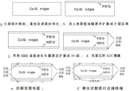
[0029] (1) First, the N-type silicon wafer is cleaned and textured, and a pyramid structure is formed on both sides of the silicon wafer;
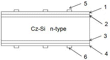
[0030] (2) Spin-coating equipment is used on the front surface of the N-type silicon wafer after texturing to coat a layer of high-concentration organic boron source with a boron content greater than 50%, so as to form a P-type doped region 2 on the surface, and make the front PN Junction; the rotation speed of the spin coating process is 5000R / min, the thickness of the boron source after coating is 5um, and the depth of the boron source doping node after diffusion is 150nm;
[0031] (3) N-type phosphorus source coating is performed on the back of the Si wafer by MBE or spin coating to form an N-type doped region 3 on the surface; the front and back of the battery are spin-coated, and MBE is used on the back to form two layers of superimposed PN Juncti...
Embodiment 2
[0039] A method for preparing double-sided solar cells based on N-type silicon wafers
[0040] (1) First, the N-type silicon wafer is cleaned and textured, and a pyramid structure is formed on both sides of the silicon wafer;
[0041] (2) Spin-coating equipment is used on the front surface of the N-type silicon wafer after texturing to coat a layer of high-concentration organic boron source with a boron content greater than 50%, so as to form a P-type doped region 2 on the surface, and make the front PN Junction; spin coating process speed 10000R / min, boron source thickness after coating is 10um, boron source doping node depth is 500nm after diffusion advance;
[0042] (3) N-type phosphorus source coating is performed on the back of the Si wafer by MBE or spin coating to form an N-type doped region 3 on the surface; the front and back of the battery are spin-coated, and the back is spin-coated to form a two-layer superposition Shaped PN junction, the battery can generate elec...
PUM
 Abstract
Description
Claims
Application Information


