
Circuit layout construction for measuring whether concave falls are generated by copper wire

A technology of layout structure and copper leads, applied in circuits, electrical components, electrical solid devices, etc., can solve problems such as complex testing process

Active Publication Date: 2011-10-26
BEIJING YANDONG MICROELECTRONICS
View PDF4 Cites 0 Cited by
  • Summary
  • Abstract
  • Description
  • Claims
  • Application Information

AI Technical Summary

Problems solved by technology

[0006] The technical problem to be solved in the present invention is to overcome the defects in the prior art that the defect testing process such as concave pits formed by copper leads after CMP is complicated, and to provide a circuit layout structure for measuring whether copper leads produce concave pits. A simple electrical measurement of the copper lead pattern of the circuit layout can tell the performance of the copper lead formed after the chemical mechanical polishing process

Method used


Image

  • Circuit layout construction for measuring whether concave falls are generated by copper wire
  • Circuit layout construction for measuring whether concave falls are generated by copper wire
  • Circuit layout construction for measuring whether concave falls are generated by copper wire

Examples


Embodiment Construction

[0015] In order to make the object, technical solution and advantages of the present invention clearer, the implementation manner of the present invention will be further described in detail below in conjunction with the accompanying drawings.

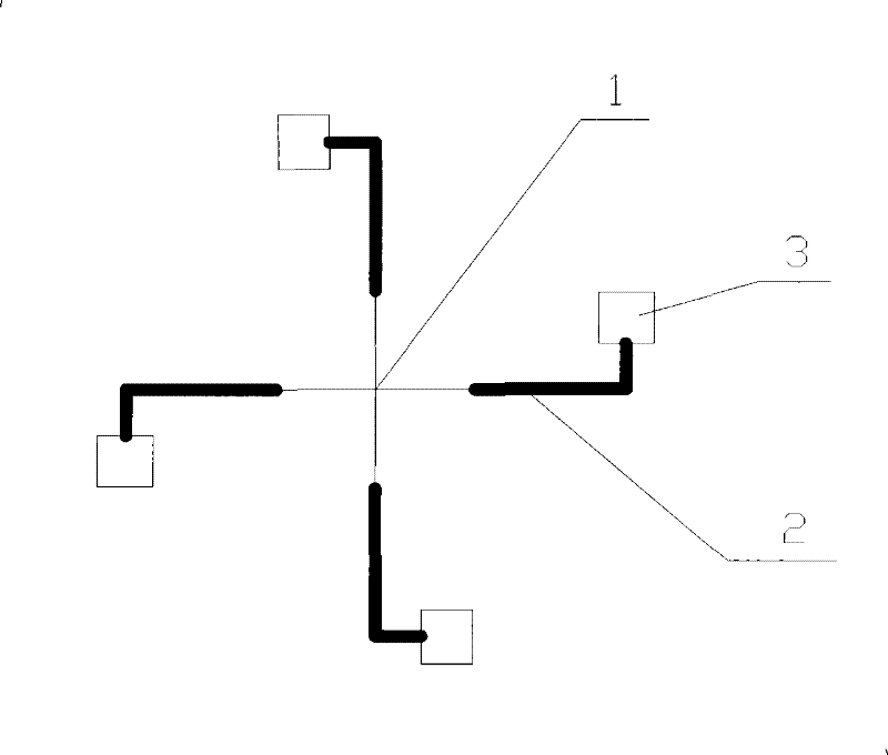
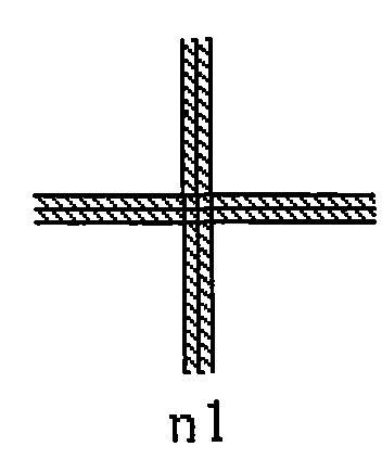
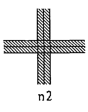
[0016] The present invention is a layout structure for testing concave pits of copper leads by an electrical testing method. The layout structure includes a set of independent copper lead cross unit arrays, and the independent cross unit array is composed of at least two mutually independent cross units. ,Such as figure 1 As shown, each independent cross unit is composed of copper leads 1 of equi-arm cross structure. The copper leads of each independent cross unit have four output terminals 2 . The copper lead groove depth of each independent cross unit is the same. The copper lead line width of each individual cross unit is different. Such as diagram 2-1 , Figure 2-2 and Figure 2-3 As shown, the independent cross unit array i...


PUM


Abstract

The invention discloses a circuit domain structure for measuring whether a copper lead wire generates a concave pit. The circuit domain structure comprises a group of independent copper lead wire cross unit arrays. The independent cross unit array is composed of at least two mutually-independent cross units; and each independent cross unit is composed of a copper lead wire with an equiarm cross structure. The invention can be used for electrically measuring whether the copper lead wire generates the concave pit during the CMP process. The invention has simple structure, small occupied domain area, and convenient laboratory measurement, and is conveniently embedded in the domain. The measurement can not be influenced by the dimension of a line by adopting the electrical method, thereby the whole chip can be conveniently measured, and the uniformity of the CMP of the chip can be better verified.

Description

technical field [0001] The invention relates to a circuit layout structure of a semiconductor device, in particular to a circuit layout structure for measuring whether concave pits are generated on copper leads. Background technique [0002] With the improvement of the manufacturing process and the continuous reduction of the device size, the interconnect delay has become a bottleneck affecting the performance of the entire circuit. In order to reduce the interconnection delay, copper with a lower resistivity is used as the metal lead. In the three-dimensional structure of multilayer wiring, ensuring that each layer can achieve global planarization is the key to realizing multilayer wiring, and the use of CMP (Chemical Mechanical Polishing Process) technology is one of the best solutions recognized all over the world. The copper leads formed by the damascene process also need to polish the excess deposited copper by CMP, leaving only the copper leads in the trench. All of ...

Claims


Application Information

Patent Timeline
Patent Type & Authority Patents(China)
IPC IPC(8): H01L23/544
Inventor 范雪梅赵超荣杜寰胡云中雒建斌
Owner BEIJING YANDONG MICROELECTRONICS
Learn More