

Double-layer glue removing method used for electron beam lithography stripping
An electron beam lithography, double-layer adhesive technology, applied in coating, optics, circuits, etc., can solve the problem of blurred internal cutting structure of double-layer adhesive, improve the peeling yield, reduce the difficulty of peeling process, and widely The effect of the application foreground
- Summary
- Abstract
- Description
- Claims
- Application Information
AI Technical Summary
Problems solved by technology
Method used
Image

Examples
Embodiment Construction
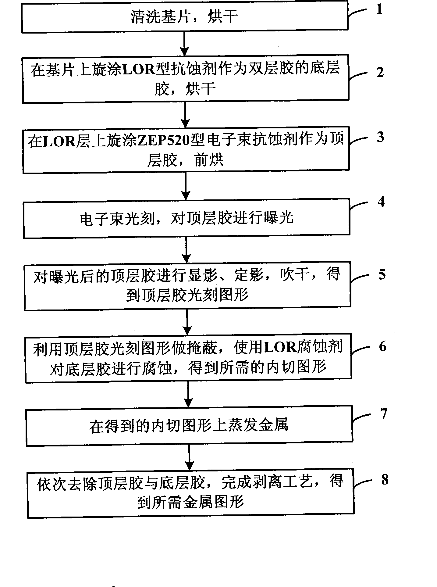
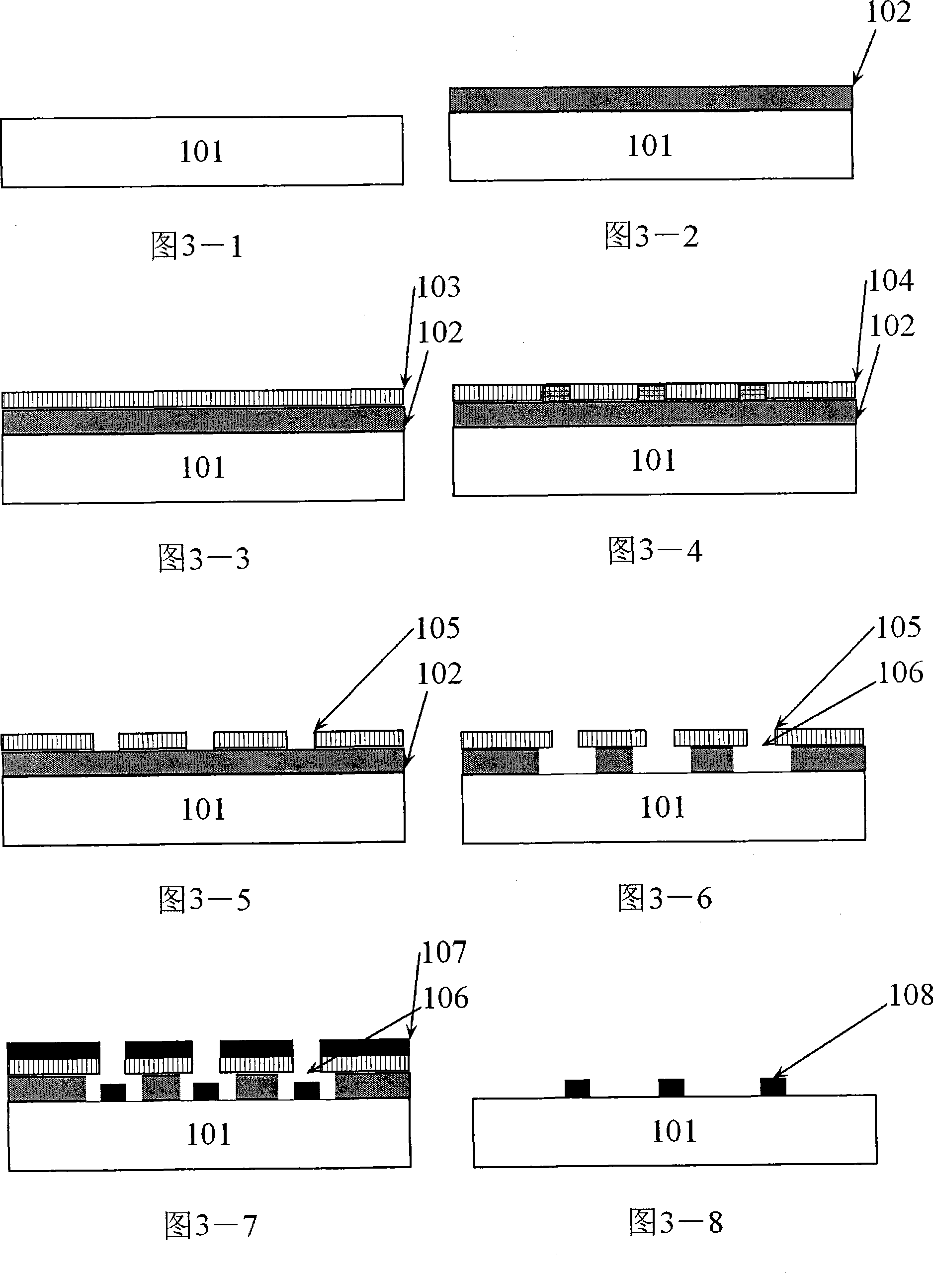
[0034] In order to make the object, technical solution and advantages of the present invention clearer, the present invention will be described in further detail below in conjunction with specific embodiments and with reference to the accompanying drawings.
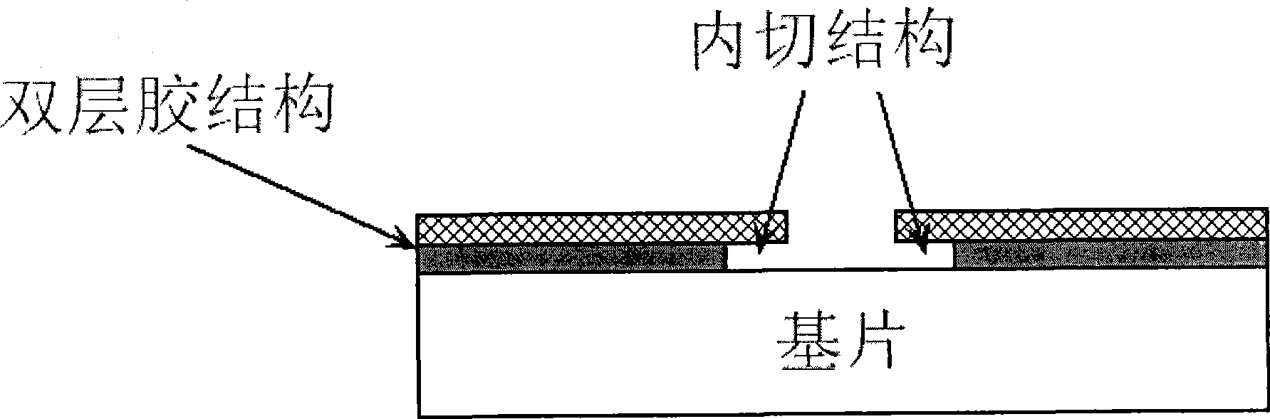
[0035] LOR (Micro Chem.Corp.) is not sensitive to electron beams, and is insoluble in PMMA / ZEP520 commonly used developer and fixer. It is an ideal choice for the bottom layer of electron beam double-layer adhesives. Therefore, the present invention uses ZEP520 as the top glue and LOR as the bottom glue, which has high innovative significance and practical value. Moreover, at present, there is no patent application for the double-layer adhesive process applied to electron beam lithography. The patent applied for (Chinese patent application number: 02123171.0) is a double-layer adhesive process for optical lithography, and the method of etching the bottom layer adhesive with O2 / HBr gas is complicated and different from the...
PUM
 Abstract
Description
Claims
Application Information