Wafer resistor element and manufacturing method thereof

A chip resistance and manufacturing method technology, applied in the direction of resistance manufacturing, electrical components, resistors, etc., can solve the problems of inconvenience, general products and methods without suitable structures and methods, etc.

Inactive Publication Date: 2009-05-13
YAGEO CORP
View PDF1 Cites 11 Cited by
  • Summary
  • Abstract
  • Description
  • Claims
  • Application Information

AI Technical Summary

Problems solved by technology

[0025] This shows that the above-mentioned existing chip resistance element and its manufacturing method obviously still have inconvenience and defects in product structure, manufacturing method and use, and need to be further improved urgently
In order to solve the above-mentioned problems, the relevant manufacturers have tried their best to find a solution, but no suitable design has been developed for a long time, and the general products and methods have no suitable structure and method to solve the above-mentioned problems. Obviously, it is a problem that relevant industry players are eager to solve.

Method used


Image

  • Wafer resistor element and manufacturing method thereof
  • Wafer resistor element and manufacturing method thereof
  • Wafer resistor element and manufacturing method thereof

Examples


Embodiment Construction

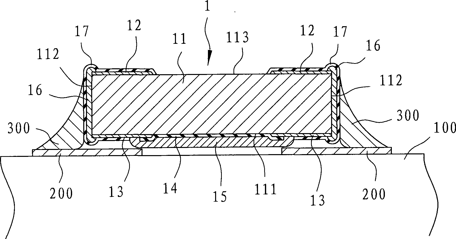
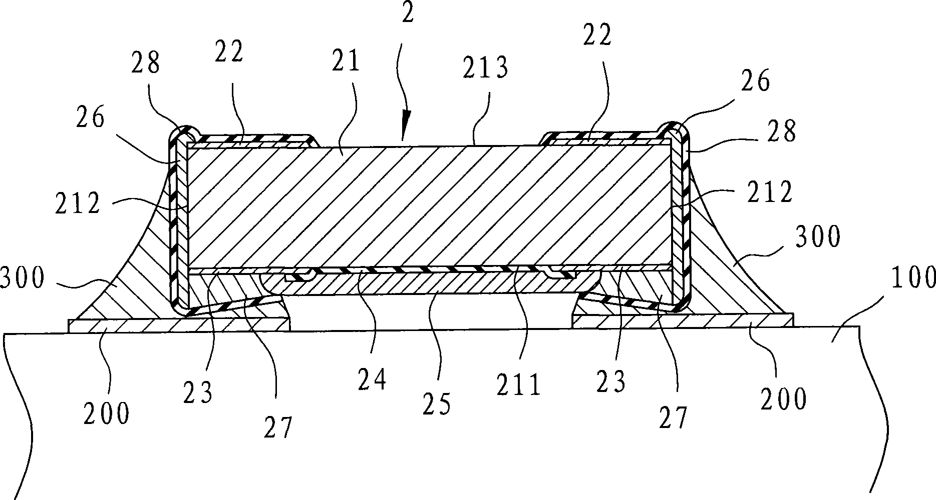
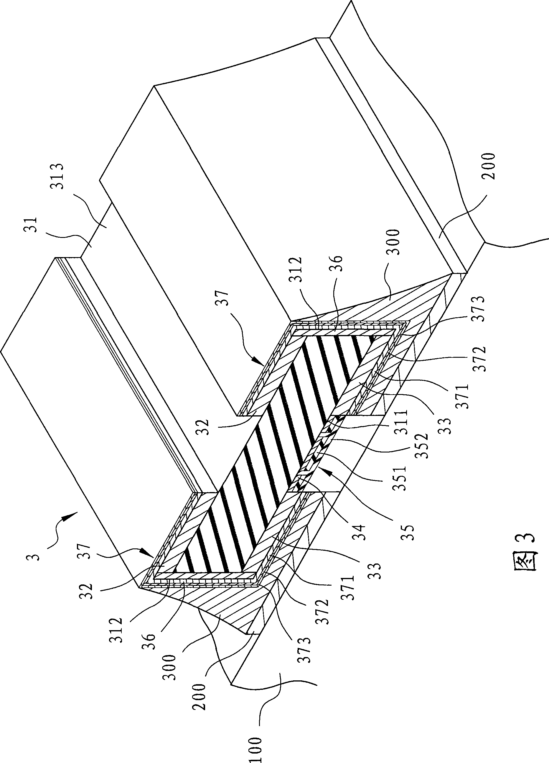
[0082] In order to further explain the technical means and effects that the present invention takes to achieve the intended purpose of the invention, below in conjunction with the accompanying drawings and preferred embodiments, the specific implementation, structure and method of the chip resistance element and its manufacturing method proposed according to the present invention will be described below. , steps, features and effects thereof are described in detail below.

[0083] The aforementioned and other technical contents, features and effects of the present invention will be clearly presented in the following detailed description of preferred embodiments with reference to the drawings. Through the description of the specific implementation mode, when the technical means and functions adopted by the present invention to achieve the predetermined purpose can be obtained a deeper and more specific understanding, but the accompanying drawings are only for reference and descr...


PUM


Abstract

The invention relates to a wafer resistance element and a preparation method thereof; wherein, the wafer resistance element comprises a substrate, two positive electrodes which are arranged on the frontal surface of the substrate, two back electrodes which are arranged on the back surface of the substrate, a resistance layer which is arranged between the two back electrodes and provided with prearranged resistance, a protection film which coats the resistance layer and is isolated from the environment, two side electrodes which are respectively arranged on two side surfaces of the substrate and are electrically connected with the positive electrodes and the back electrodes at the same side respectively, and two layers of coatings which form three layers of coats from above the surfaces of the positive electrodes, the side electrodes and the back electrodes at the same side and comprise the main compositions of copper, nickel and tin. The invention also provides the method used for preparing the wafer resistance element. The wafer resistance element and the preparation method thereof take the copper, the nickel and the tin as main materials to form the coatings with simple preparation process, lead the element to be easily and correctly positioned on a soldering pad by liquid solder tin and to be bonded with the solder tin into a whole excellently, reduce the electron circulation path from the element to the soldering pad, and lead the element to have large power application and to provide precise micro-resistance values.

Description

technical field [0001] The invention relates to a passive element and its manufacturing method, in particular to a chip resistance element with micro-ohm (micro-Ω) level resistance and its manufacturing method. Background technique [0002] see figure 1 Shown is a cross-sectional view illustrating a conventional chip resistor element and its structure welded on a pad of a laminated circuit board. The chip resistance element is a passive element welded on a laminated circuit board 100 (PCB), and is used to provide a resistance value in the micro-ohm scale. The chip resistance element 1 includes a substrate 11 , two positive electrodes 12 , two back electrodes 13 , a resistive layer 14 , a protection layer 15 , two side electrodes 16 , and two plating layers 17 . [0003] The base material 11 is made of insulating material and is shaped like a rectangular plate. It has a back side 111 , two side surfaces 112 extending upwards from opposite sides of the back side 111 , and a ...

Claims


Application Information

Patent Timeline
Patent Type & Authority Applications(China)
IPC IPC(8): H01C7/00H01C17/00
Inventor 陈木元吴文丰章启斌简高柏
Owner YAGEO CORP
Why Eureka
Try Eureka