Pulsed growth of gan nanowires and applications in group III nitride semiconductor substrate materials and devices

A technology of nanowires and semiconductors, applied in the field of semiconductor nanowires and semiconductor nanowire active devices, can solve the problems of reducing the crystallization quality and limitations of nanostructures

Active Publication Date: 2009-05-27
新墨西哥大学雨林创新公司
View PDF0 Cites 86 Cited by
  • Summary
  • Abstract
  • Description
  • Claims
  • Application Information

AI Technical Summary

Problems solved by technology

This reduces the crystalline quality of the nanostructures formed, which limits their applications

Method used


Image

  • Pulsed growth of gan nanowires and applications in group III nitride semiconductor substrate materials and devices
  • Pulsed growth of gan nanowires and applications in group III nitride semiconductor substrate materials and devices
  • Pulsed growth of gan nanowires and applications in group III nitride semiconductor substrate materials and devices

Examples


Embodiment Construction

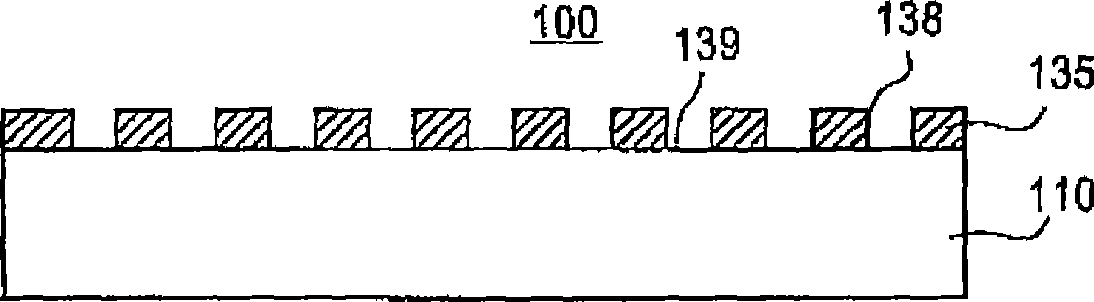
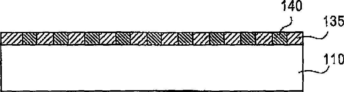
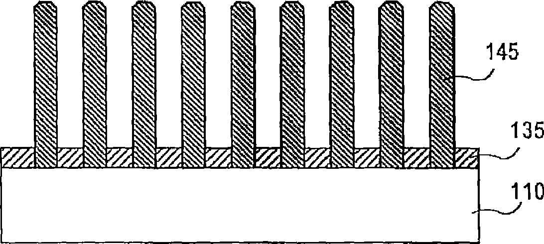
[0027] Reference will now be made in detail to the exemplary embodiments of the present invention, examples of which are illustrated in the accompanying drawings. Wherever possible, the same reference numbers will be used throughout the drawings to refer to the same or like parts. In the following description, reference is made to the accompanying drawings which form a part hereof, and in which is shown by way of illustration certain typical embodiments in which the invention may be practiced. These embodiments are described in sufficient detail to allow those skilled in the art to practice the invention, and it is to be understood that other embodiments may be utilized and changes may be made without departing from the scope of the invention. The following description is thus merely exemplary.

[0028] While the invention has been described with respect to one or more implementations, changes and / or modifications to the examples shown may be made without departing from the s...


PUM

PropertyMeasurementUnit
diameteraaaaaaaaaa
distanceaaaaaaaaaa
lengthaaaaaaaaaa

Abstract

Exemplary embodiments provide semiconductor devices including high-quality (i.e., defect free) group III-N nanowires and uniform group III-N nanowire arrays as well as their scalable processes for manufacturing, where the position, orientation, cross-sectional features, length and the crystallinity of each nanowire can be precisely controlled. A pulsed growth mode can be used to fabricate the disclosed group III-N nanowires and / or nanowire arrays providing a uniform length of about 10 nm to about 1000 microns with constant cross-sectional features including an exemplary diameter of about 10-1000 nm. In addition, high-quality GaN substrate structures can be formed by coalescing the plurality of GaN nanowires and / or nanowire arrays to facilitate the fabrication of visible LEDs and lasers. Furthermore, core-shell nanowire / MQW active structures can be formed by a core-shell growth on the nonpolar sidewalls of each nanowire.

Description

[0001] government rights [0002] This invention was made with government support under Contract No. HR0011-05-1-0006 awarded by the Defense Advanced Research Projects Agency / Army Research Institute, and Contract No. F49620-03-1-0013 awarded by the Air Force Institute of No. FA9550-06-1-0001 down to achieve. The government may have certain rights in this invention. [0003] related application [0004] This application claims U.S. Provisional Patent Applications Serial No. 60 / 780,833, filed March 10, 2006, Serial No. 60 / 798,337, filed May 8, 2006, Serial No. 60 / 808,153, filed May 25, 2006, and Priority of Serial No. 60 / 889,363 filed February 12, 2007, which is hereby incorporated by reference in its entirety. technical field [0005] The present invention generally relates to semiconductor materials, devices, and manufacturing methods thereof, and in particular to semiconductor nanowires and semiconductor nanowire active devices. Background technique [0006] Nanowires c...

Claims


Application Information

Patent Timeline
Patent Type & Authority Applications(China)
IPC IPC(8): H01L21/20
Inventor S·M·赫尔西X·王X·孙
Owner 新墨西哥大学雨林创新公司
Why Eureka
Try Eureka