Liquid crystal display device, array substrate and method for repairing defects thereof

A technology for liquid crystal display devices and array substrates, applied in nonlinear optics, instruments, optics, etc., can solve the problems of low production yield, and achieve the effects of improving yield, improving performance, and avoiding scrapping

Active Publication Date: 2009-06-03
KUSN INFOVISION OPTOELECTRONICS
View PDF0 Cites 28 Cited by
  • Summary
  • Abstract
  • Description
  • Claims
  • Application Information

AI Technical Summary

Problems solved by technology

[0010] The invention provides a liquid crystal display device, an array substrate and a defect repairing method thereof, which can solve the problem of low production yield in the existing array substrate due to the increase in the number of data lines

Method used


Image

  • Liquid crystal display device, array substrate and method for repairing defects thereof
  • Liquid crystal display device, array substrate and method for repairing defects thereof
  • Liquid crystal display device, array substrate and method for repairing defects thereof

Examples


no. 1 example

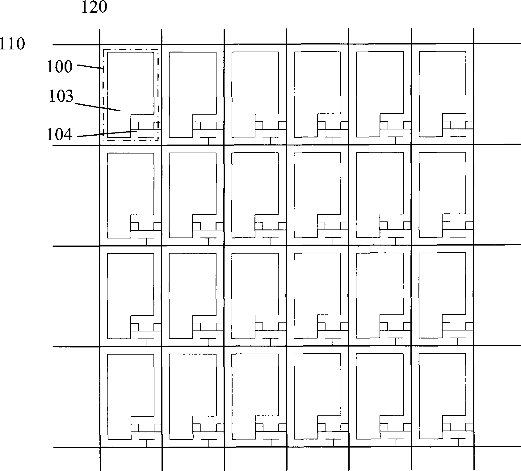
[0050] Figure 4 It is a schematic diagram of the array substrate of the liquid crystal display device in the first embodiment of the present invention, such as Figure 4 As shown, the array substrate includes scan lines 410 , data lines 420 arranged across the scan lines 410 , pixel units 400 , pixel electrodes 403 and transistors 404 disposed in the pixel units 400 .

[0051] Among them, its scan line 410 (including Figure 4 G(m) and G(m+2) shown in ) and data line 420 (including Figure 4 D(n), D(n+1)...etc. shown in image 3 The same as shown in , and will not be repeated here.

[0052] Such as Figure 4 As shown, the array substrate also includes a first repair line 451 and a second repair line 452 located in different layers, and the first repair line 451 is also in a different layer from the data line 420, and the second repair line 452 It also has a different layer from the scan line 410 . In this embodiment, for the convenience of manufacture, the first repair ...

no. 2 example

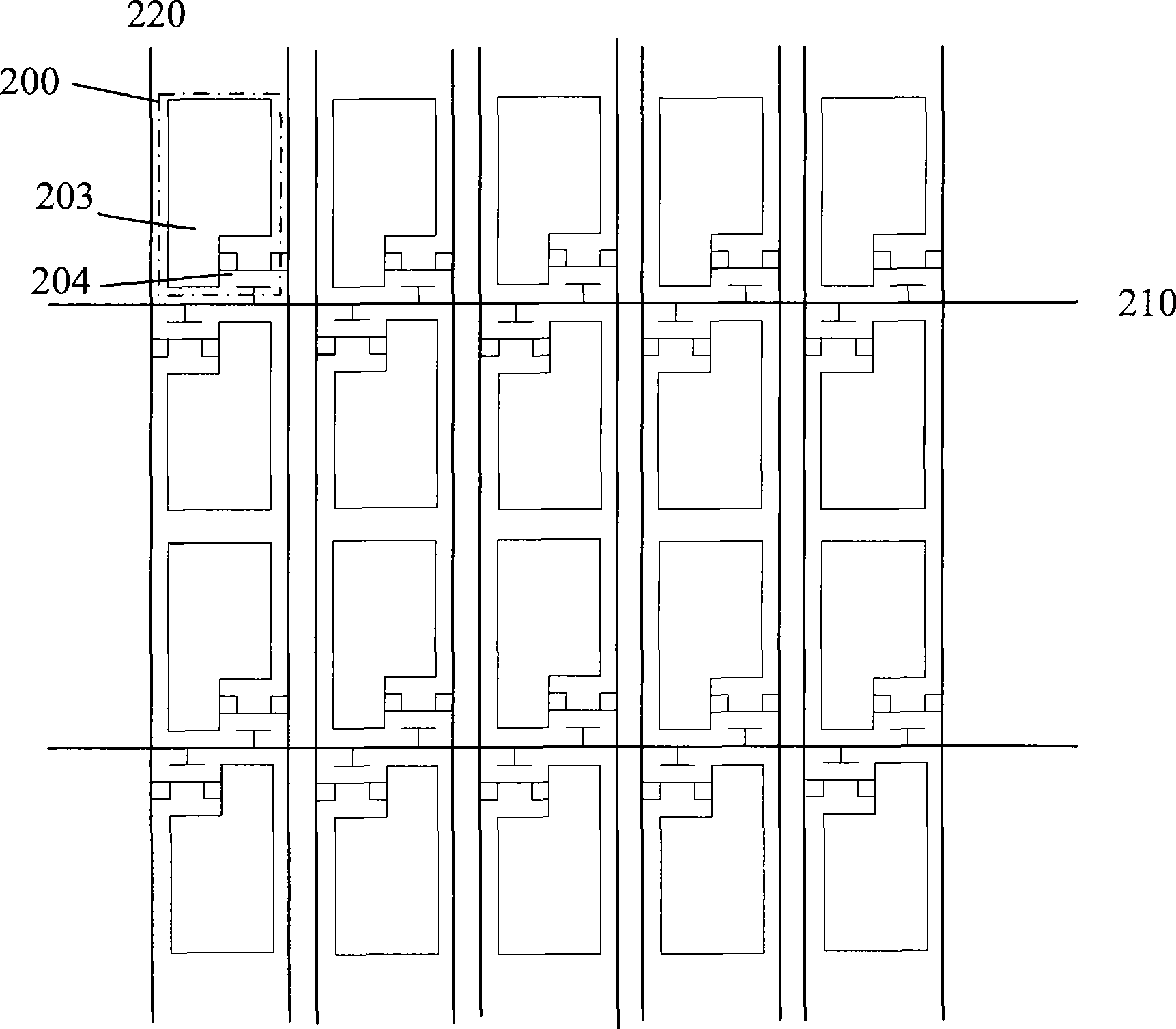
[0060] Figure 5 It is a schematic diagram of the array substrate of the liquid crystal display device in the second embodiment of the present invention, such as Figure 5 As shown, the array substrate includes scan lines 510 , data lines 520 arranged across the scan lines 510 , pixel units 500 , pixel electrodes 503 and transistors 504 disposed in the pixel units 500 .

[0061] Among them, its scan line 510 (including Figure 5 G(m) and G(m+2) shown in ) and data line 520 (including Figure 5 D(n), D(n+1)...etc. shown in ) and each pixel unit 500 are connected with Figure 5 The same as shown in , and will not be repeated here.

[0062] Such as Figure 5 As shown, the array substrate further includes a first repair line 551 and a second repair line 552 located in different layers. Preferably, the first repair line 551 and the scanning line 510 can be arranged in the same layer, and the second repair line 551 can be arranged in the same layer. 552 and the data line 520 ar...

no. 3 example

[0080] This embodiment introduces in detail the specific repairing method of the array substrate with repaired lines of the present invention.

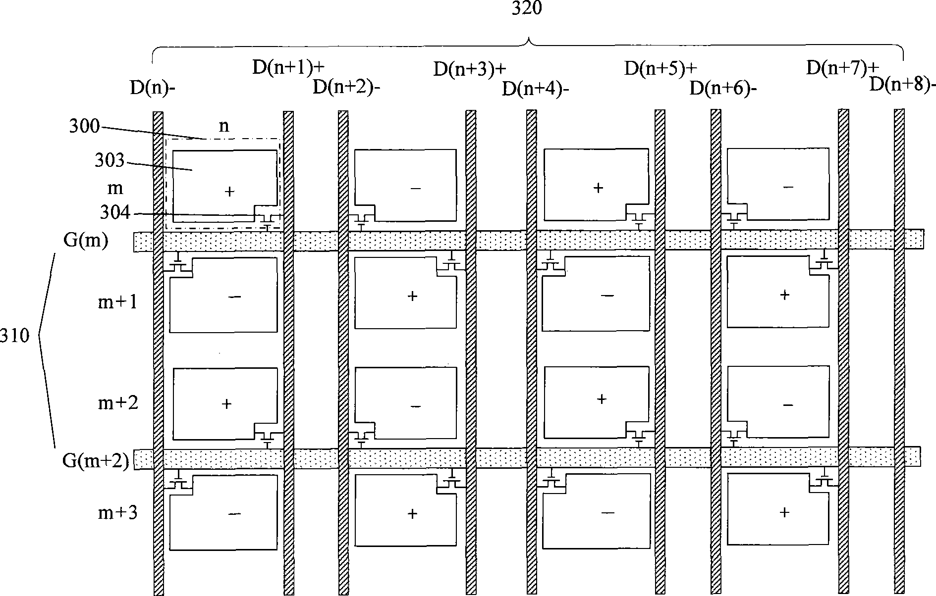
[0081] Figure 7 It is a flow chart of the method for repairing defects of the array substrate in the third embodiment of the present invention. FIG. 8 is a schematic diagram of the array substrate of the liquid crystal display device repaired by the repair method in the third embodiment of the present invention. The following combines Figure 7 and FIG. 8 specifically introduce the repairing method of this embodiment.

[0082] Step 701: Detect and determine the defects of the data lines on the array substrate. As shown in FIG. 8 , open circuit defects 841 and 842 appear on the data lines D(n+3) and D(n+5), respectively. If the array substrate does not have the repaired circuit of the present invention, the two columns of pixel units cannot display normally, and the array substrate can only be scrapped. However, the array substrate...


PUM


Abstract

The invention discloses an array substrate of a liquid crystal display device, which comprises scanning wires, data wires, pixel cells as well as pixel electrodes and transistors which are arranged in the pixel cells, wherein every two lines of pixel cells in the array substrate can configure one scanning wire, and every one row of pixel cells configures two data wires; the array substrate also comprises first repairing wires and second repairing wires, which are arranged in different layers, and the first repairing wires are arranged between every two adjacent rows of pixel cells, are extended along the direction of the data wires and are broken on each of the crossed parts of the first repairing wires and the scanning wires; the second repairing wires are arranged on the broken parts of the first repairing wires, stripe over the scanning wires corresponding to the broken parts and extend along the direction of the data wires. The invention also discloses the liquid crystal display device applying the array substrate as well as a repairing method used for the array substrate. The liquid crystal display device, the array substrate and the defect repairing method thereof can solve the problem of lower yield caused by the defects of the data wires.

Description

technical field [0001] The invention relates to the technical field of semiconductor manufacturing, in particular to a liquid crystal display device with a repaired circuit, an array substrate and a defect repairing method thereof. Background technique [0002] Liquid Crystal Displays (LCDs) have the advantages of lightness, thinness, and low power consumption, and are widely used in modern information equipment such as computers, mobile phones, and personal digital assistants. [0003] figure 1 It is a schematic diagram of an array substrate of an existing liquid crystal display device, such as figure 1 As shown, the array substrate includes scanning lines 110; data lines 120 intersecting the scanning lines; pixel electrodes 103 and thin films arranged in the pixel unit 100 formed by the intersections of the scanning lines 110 and the data lines 120 A transistor 104 (Thin Film Transistor, TFT for short). Wherein, the gate of the thin film transistor 104 is electrically c...

Claims


Application Information

Patent Timeline
Patent Type & Authority Applications(China)
IPC IPC(8): G02F1/1362G02F1/13
Inventor 钟德镇廖家德
Owner KUSN INFOVISION OPTOELECTRONICS
Why Eureka
Try Eureka