Plasma treatment apparatus and shield ring thereof

A plasma and plasma-resistant technology, applied in plasma, semiconductor/solid-state device manufacturing, gaseous chemical plating, etc., can solve problems such as plasma leakage, increased manufacturing costs, and the length of the exhaust channel 163 cannot be too long , to achieve the effects of improved restraint effect, extended service life and outstanding technical effect

Active Publication Date: 2009-06-10
BEIJING NAURA MICROELECTRONICS EQUIP CO LTD
View PDF0 Cites 17 Cited by
  • Summary
  • Abstract
  • Description
  • Claims
  • Application Information

AI Technical Summary

Problems solved by technology

[0012] However, the above-mentioned mean free path is only an average value, and the difference between the actual free paths of each specific charged particle is relatively large, and the length of the exhaust channel 163 can only be greater than the free paths of some charged particles forever; 1, the length of the exhaust passage 163 cannot be too long; moreover, as the length of the exhaust passage 163 increases, its manufacturing cost will increase significantly
[0013] Under the influence of the above-mentioned factors, the free path of the charged particles occupying a considerable proportion will be greater than the length of the exhaust passage 163, so it is likely not to collide with the inner wall of the exhaust passage 163, and pass through the straight passage formed by the exhaust passage 163. directly through the shielding ring 16, resulting in plasma leakage
[0014] Therefore, the shielding ring 16 in the prior art cannot effectively confine the plasma, resulting in that the internal structure of the plasma processing device 1 is easily damaged, and its service life is also significantly shortened.

Method used


Image

  • Plasma treatment apparatus and shield ring thereof
  • Plasma treatment apparatus and shield ring thereof
  • Plasma treatment apparatus and shield ring thereof

Examples


Embodiment Construction

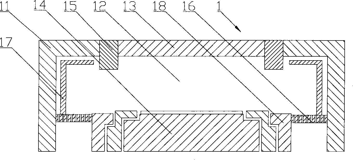
[0043] The core of the present invention is to provide a plasma shielding ring capable of effectively confining plasma, and a plasma processing device using the plasma shielding ring.

[0044] In order to enable those skilled in the art to better understand the solution of the present invention, the present invention will be further described in detail below in conjunction with the accompanying drawings and specific embodiments.

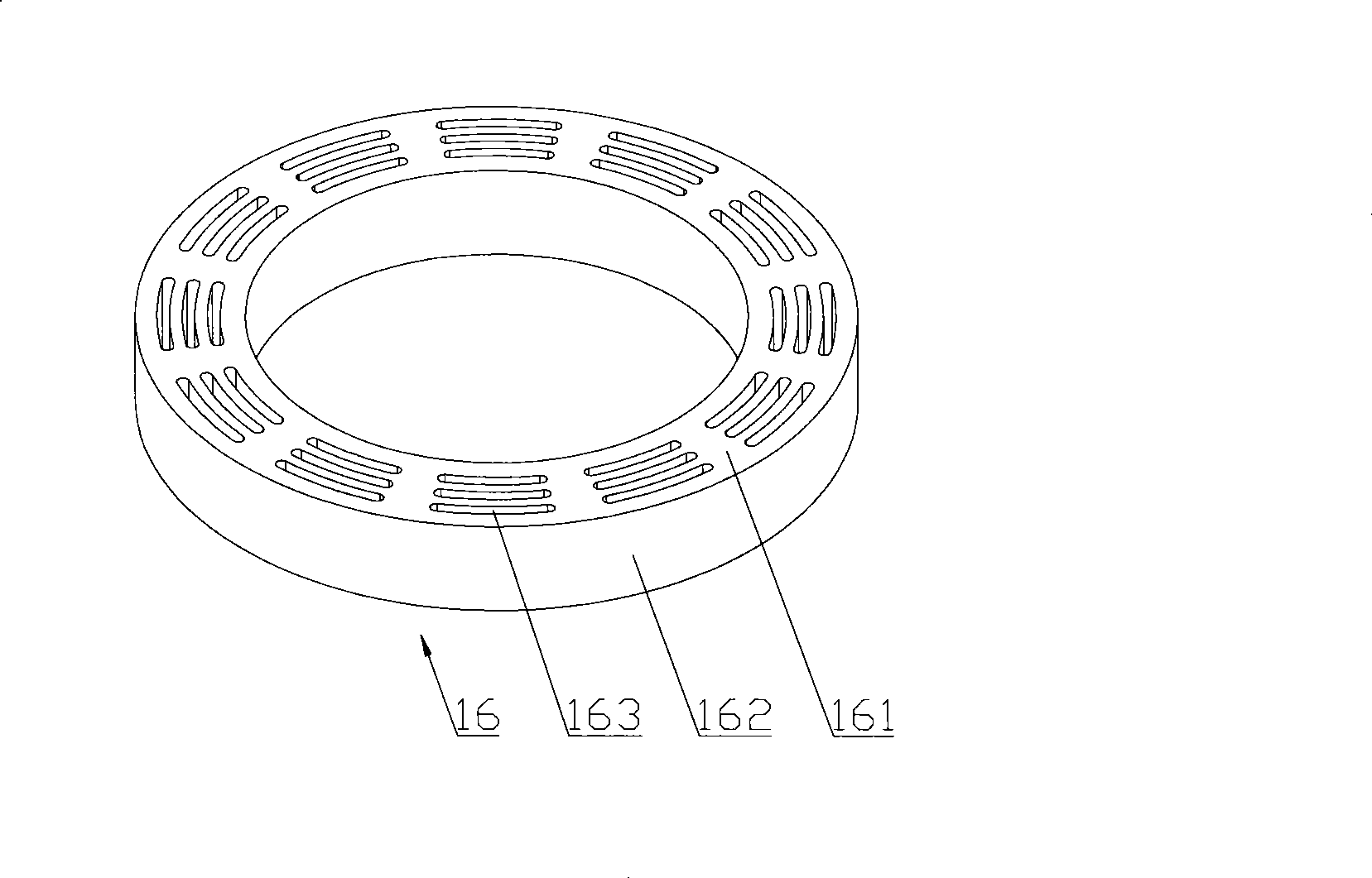
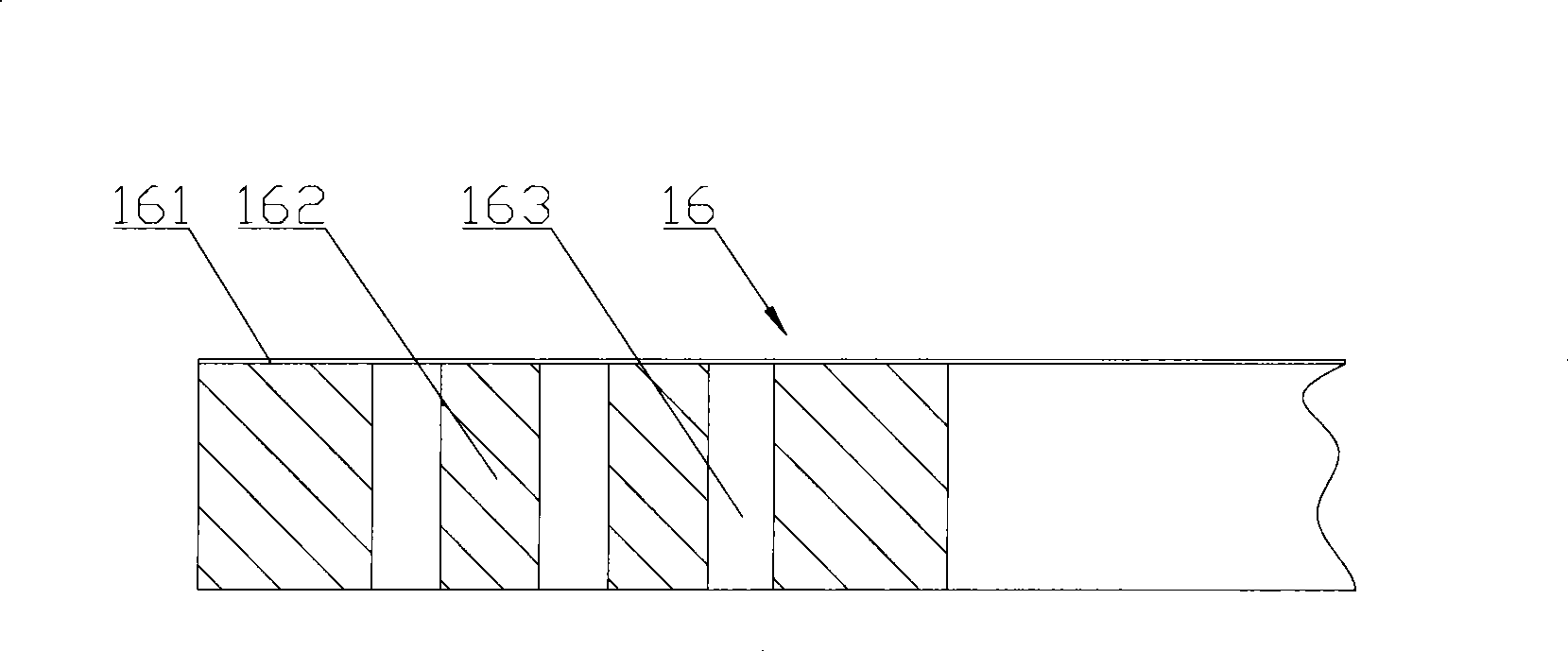
[0045] Please refer to Figure 4 , Figure 4 It is a partial cross-sectional schematic diagram of the first specific implementation manner of the shielding ring provided by the embodiment of the present invention.

[0046] In the first specific implementation mode, the shielding ring 2 provided by the embodiment of the present invention is generally a cylinder with a circular cross-section, including upper and lower layers, and the upper layer is an insulating layer 21, and its material can specifically be quartz, Ceramic and Si 3 N 4 and other c...


PUM


Abstract

The invention discloses a plasma shielding ring, which comprises an upper layer and a lower layer connected fixedly and integrally, wherein the upper layer is a plasma-proof insulating layer (21), and the lower layer is a conductor layer (22). At least one axially extended exhaust passage (23) penetrates the insulating layer (23) and the conductor layer (21), and the exhaust passage (23) is a bent passage. The invention also discloses a plasma processing device comprising the plasma shielding ring (2). Under the condition that the exhaust passage (23) is the bent passage, most of charged particles inevitably collide with the bent inner wall of the bent passage, so as to lose carried electric charge, and be converted into harmless neutral particles. Therefore, the plasma shielding ring (2) improves inhibiting effect on plasma remarkably; and the internal structure of the plasma processing device is not easy to be damaged, so the service life of the plasma processing device is remarkably prolonged.

Description

technical field [0001] The invention relates to semiconductor processing equipment, in particular to a plasma shielding ring of a plasma processing device. The invention also relates to a plasma processing device using the plasma shielding ring. Background technique [0002] Plasma processing equipment is processing equipment widely used in the field of semiconductor manufacturing. [0003] Please refer to figure 1 , figure 1 It is a schematic structural diagram of a typical plasma processing device in the prior art. [0004] The plasma processing apparatus 1 generally includes a housing 11 having a reaction chamber 12 therein. The top and bottom of the reaction chamber 12 are respectively provided with an upper pole plate 13 and a lower pole plate 14 correspondingly, and the upper pole plate 13 is isolated from the housing 11 by an insulating member 15; the top of the lower pole plate 14 can support the Processed parts. As we all know, the above-mentioned workpieces s...

Claims


Application Information

Patent Timeline
Patent Type & Authority Applications(China)
IPC IPC(8): H01L21/00H01L21/02H01L21/205H01L21/3065H01L21/31H01L21/311H01L21/3205H01L21/3213H01J37/32H05H1/00H05H1/46C23C16/44C23C16/513C23F4/00
CPCH01J37/32642H01J37/32495H01L21/67069H01J37/32623
Inventor 南建辉宋巧丽
Owner BEIJING NAURA MICROELECTRONICS EQUIP CO LTD
Why Eureka
Try Eureka